|
|
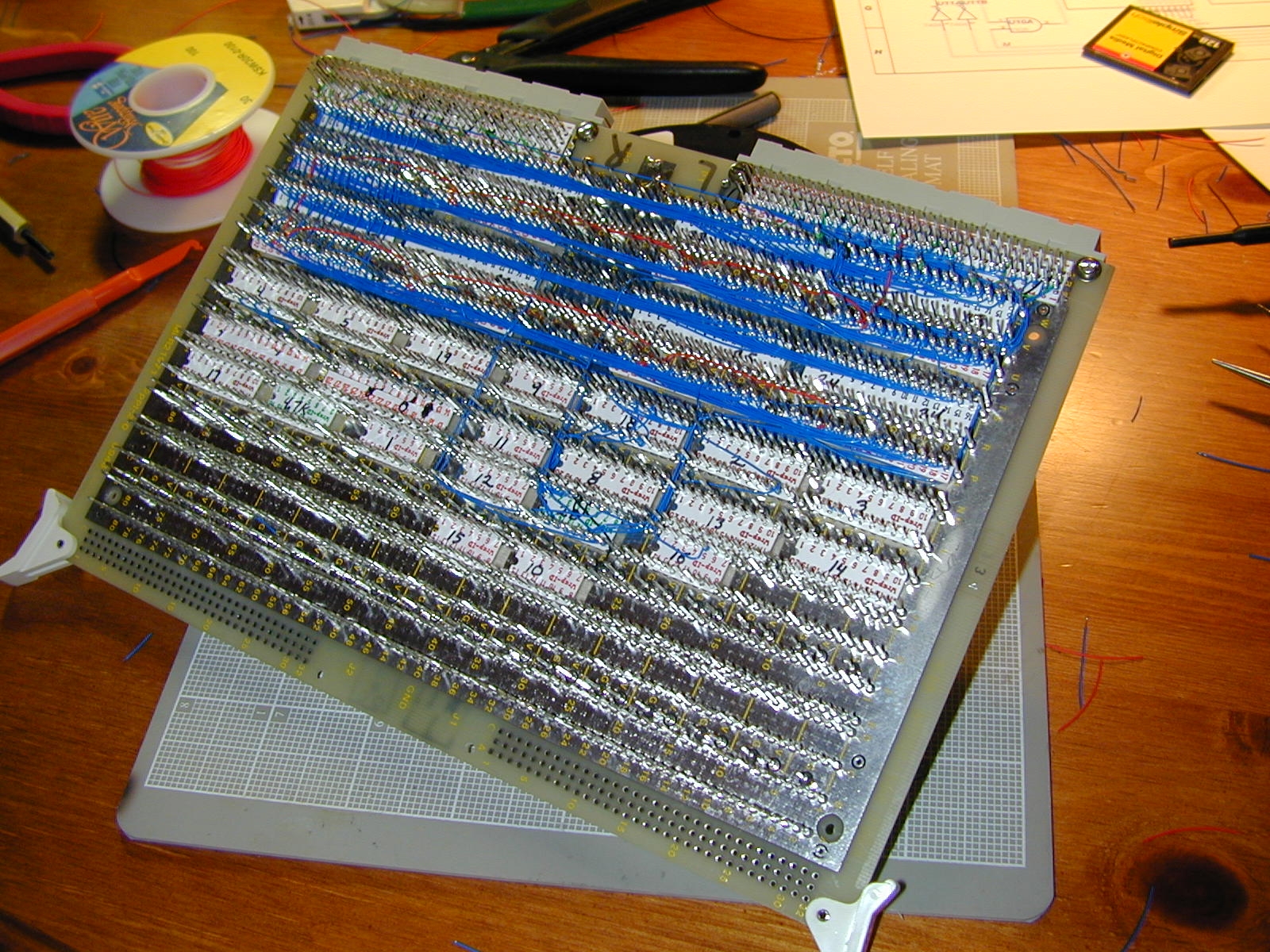
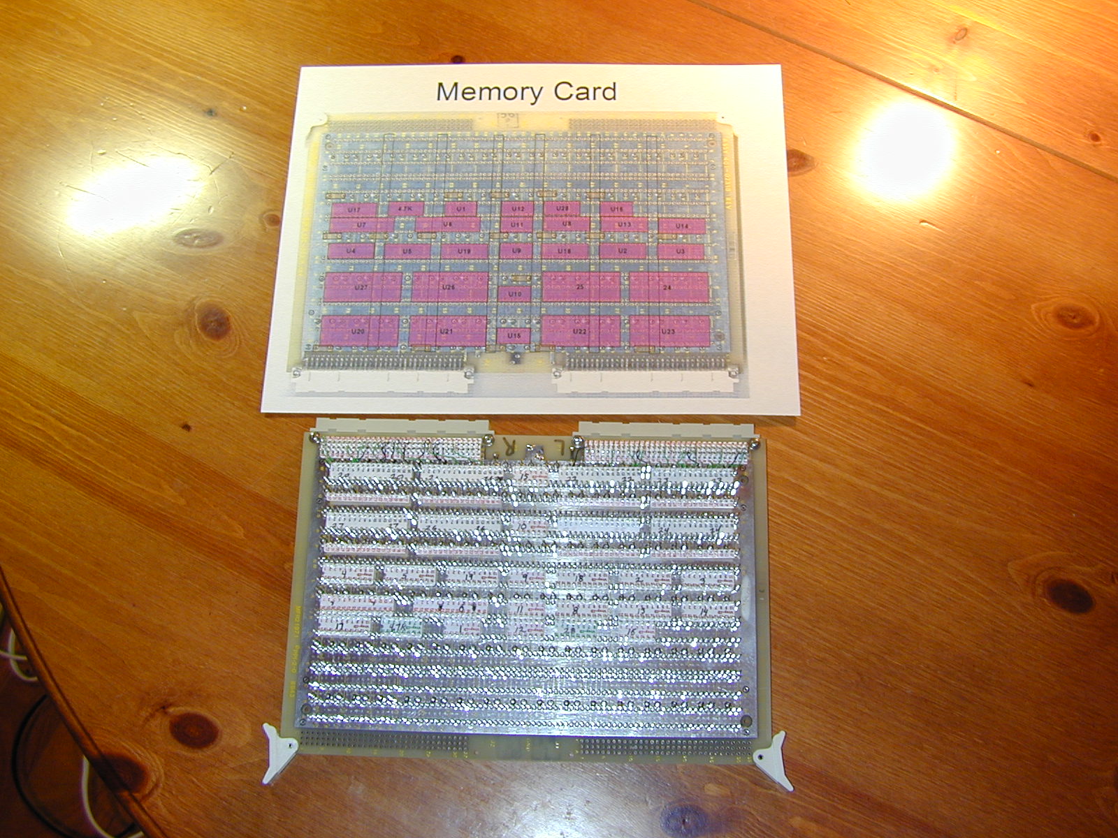
Memory Card construction [completed 2/9/2004]2/9/2004Had my testing session, and decided to call the card compete at this time. I didn't test it with the probe quite as well as I tested the front panel logic card, but my problem what that to do the comprehensive testing I had in mind, I'd need a lot more of those wires with clips on the end. For this card, there are a lot of signals that combine to determine who is driving what bus, and in which direction. I did basic testing for all of the big groupings, but typically only tested one bit of output per package. I'm not going to skip the testing, but rather defer it until the device card is complete. Once I have the device card (and a couple of banks of DIP switches on the temporary front panel assembly, I will be able to much more easily test the memory functionality. So, I'm declaring the card complete, but will perform additional tests in conjuction with the device card. Ship it. 2/8/2004Okay, the memory card is "complete" again. I added the new wiring the for bi-directional bus drivers and associated control signal tweaking. That went pretty quick. Fortunately, I thougt it best to go ahead and use the continuity checker to test every single connection on the board, as the number of changes left me somewhat less than confident that all was right with the world. Glad I did. I found one silly error (that would have been caught fairly quickly - I got the backplane pin wrong for L_MAR1). However, I also found four somewhat unsettling errors: wires which looked just fine, but were broken inside of the insulation. All four were in the address bus wiring in the SRAM, and further, all four were wires that bridged the big gap in the middle. I'm not sure how they broke - whether I did it at wrap time, or the breaks were caused by stress of subsequent wires. I'm guessing the latter. From here on out I'm going to be more careful about leaving slack. I probably went a bit overboard in my efforts to avoid a loose rat's nest. I'm also going to continuity check every connection. It was mind-numbingly boring and took a long time, but it would have taken much longer to track those things down later. Next up is live testing. With the board powered up, I believe I can test a lot using my logic probe and logic pulser. I will save some of the more interesting SRAM testing for when I have the device board built. Hope to start layout of that board within a few days. My goal is to be in a position to build and test the control board during the week I'm taking off between jobs (Feb 20-Mar 1). 2/7/2004Well, it's not finished after all. While preparing for testing, I realized that a recent bug fix I'd made introduced another serious defect. I had originally neglected to buffer the output of the page table where it drives the high order 11 address bus bits. I noticed this a while back and inserted a pair of 74F244 bus drivers between the page table SRAM and the address bus. In doing so, I somehow neglected to consider that fact that the data output of the page table SRAM needs to not only be read, but written with the page table entries. 74F244s are one-way bus drivers - and left me without the ability to write to page table memory. My biggest mistake, though, was laziness. After making the change, I decided it trivial enough that it wasn't worth updating my simulator. Had I updated the simulator, my error would have been caught and corrected long before I started wiring things up. So, here's the result:
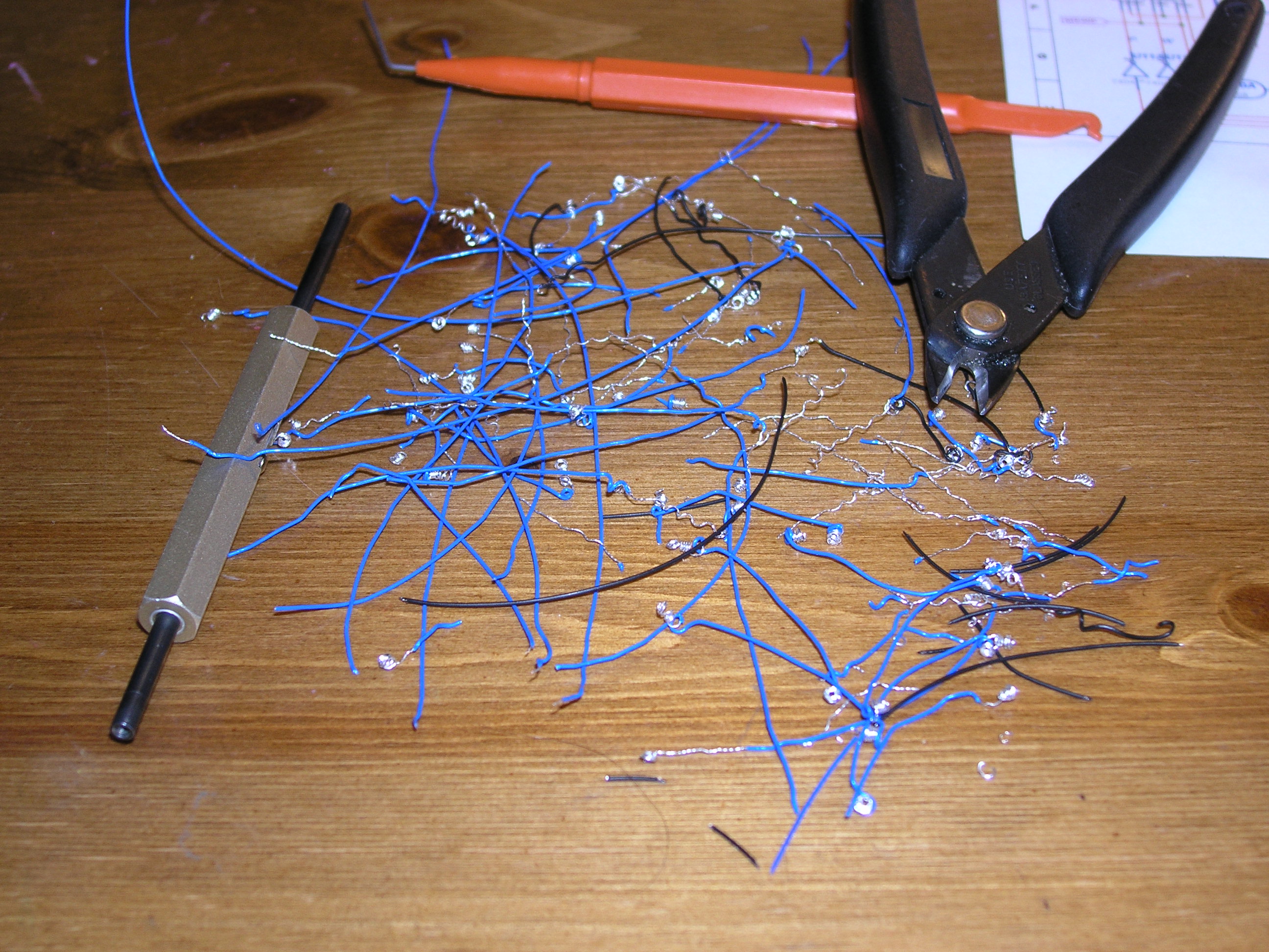
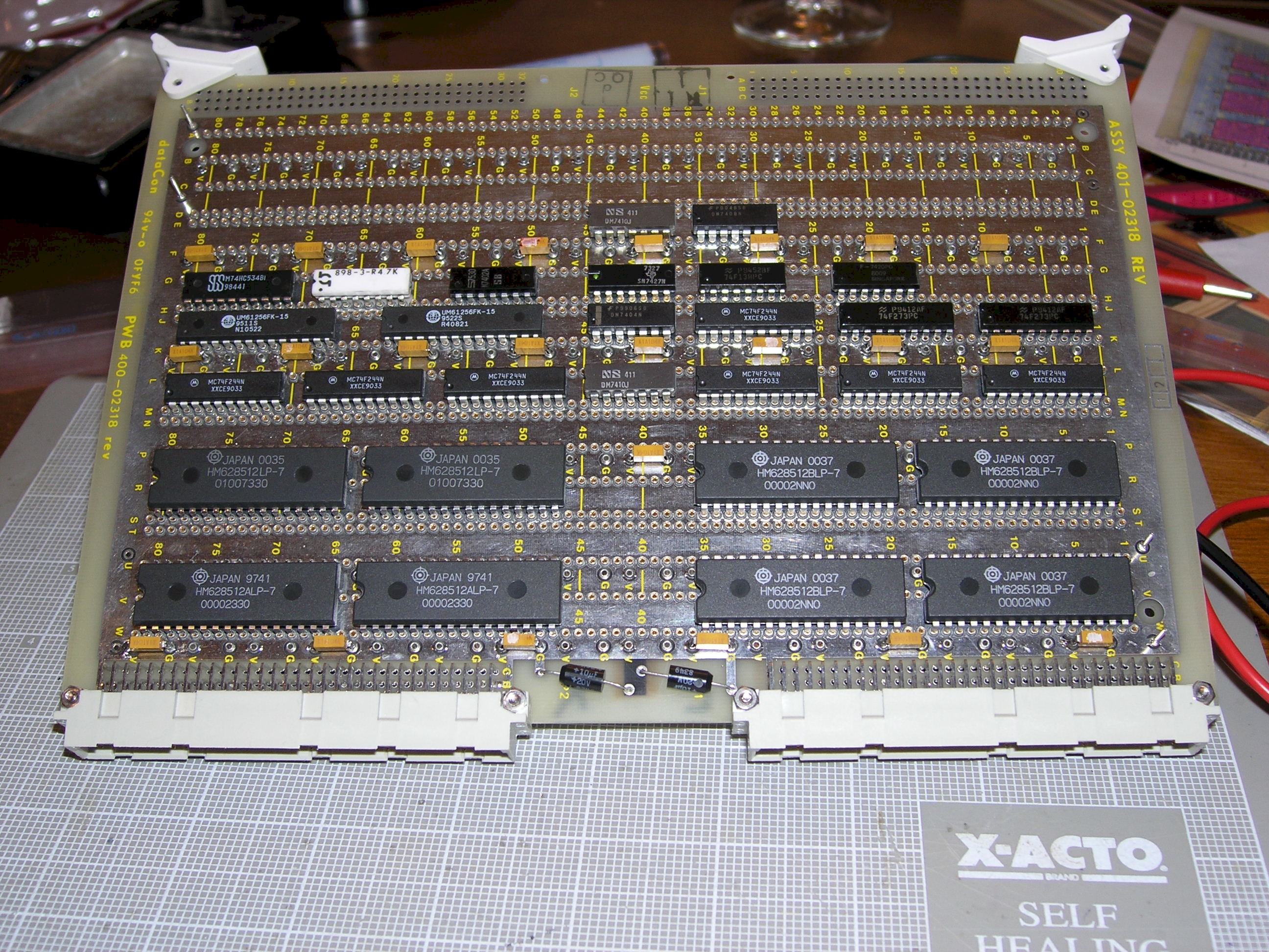
In order to fix this, I am having to replace U18 and U19 with 74F245 bi-directional bus drivers. That means yanking out a bunch of wires, which turns out to be a lot more difficult and danger-prone than you might think. Unwrapping often results in tiny wire fragments breaking off, and I had quite of bit of difficulty tracing the right wires to remove when they went through some of my tight bundles. I've completed removing wires, and I hope I haven't damaged anything. I'll add the new wires next session. Ouch. 2/6/2004Finished the memory card construction. Soldering in the bypass caps went a little better this time. My new 40 watt iron was certainly enough to get good solder connections, but I found it a bit unwieldy. I ended up using my old Ungar set at its highest temperature. After the caps were down, I checked for cold joints - and found a few. Fixed them with the big 40-watt iron. It went well. Here's a view of the component side:
And a view just after getting the bypass caps in:
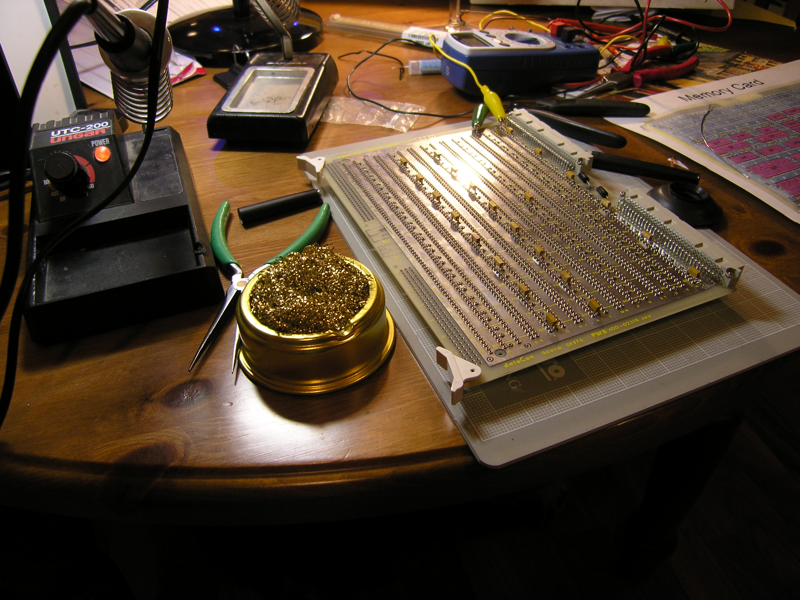
Testing of this card is going to be a bit tricky, and very repetitive. I'm temped to put it off until the device card in complete. With the device card in, I can use the front panel switches to load, store and view memory. However, I think it best if I go ahead and do all the testing I can now before starting on the next board. I'll try to find some testing time this weekend. I did, however, apply power to the board briefly. It draws about 600mA, about what I expected. 2/3/2004Discovered that if an expensive digital camera is dropped from about 5 feet onto concrete, it is quite possible to destroy it. Oh well, it was 4 years old. So, got a new camera and haven't quite figured out how to use it. But, here goes:
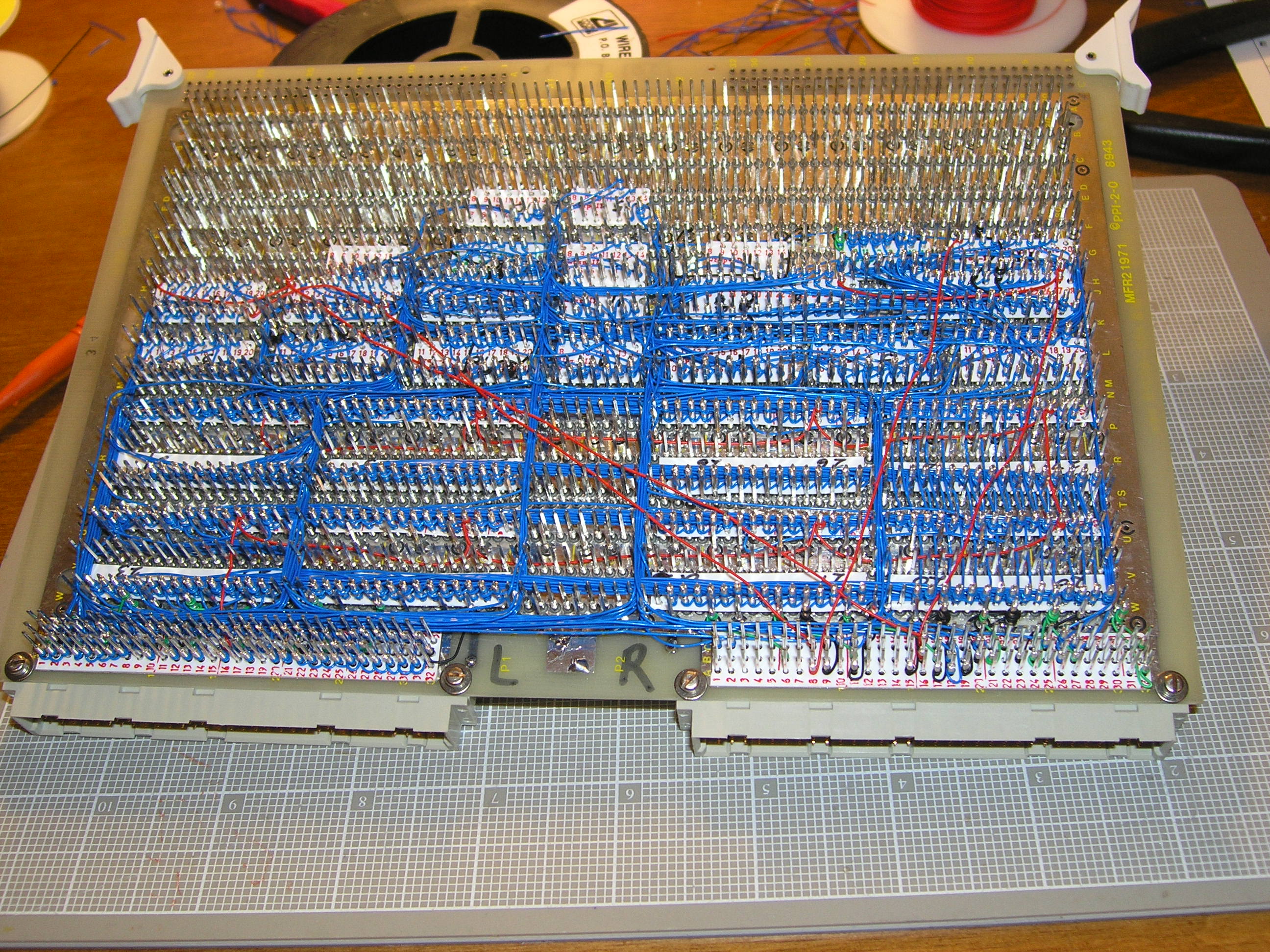
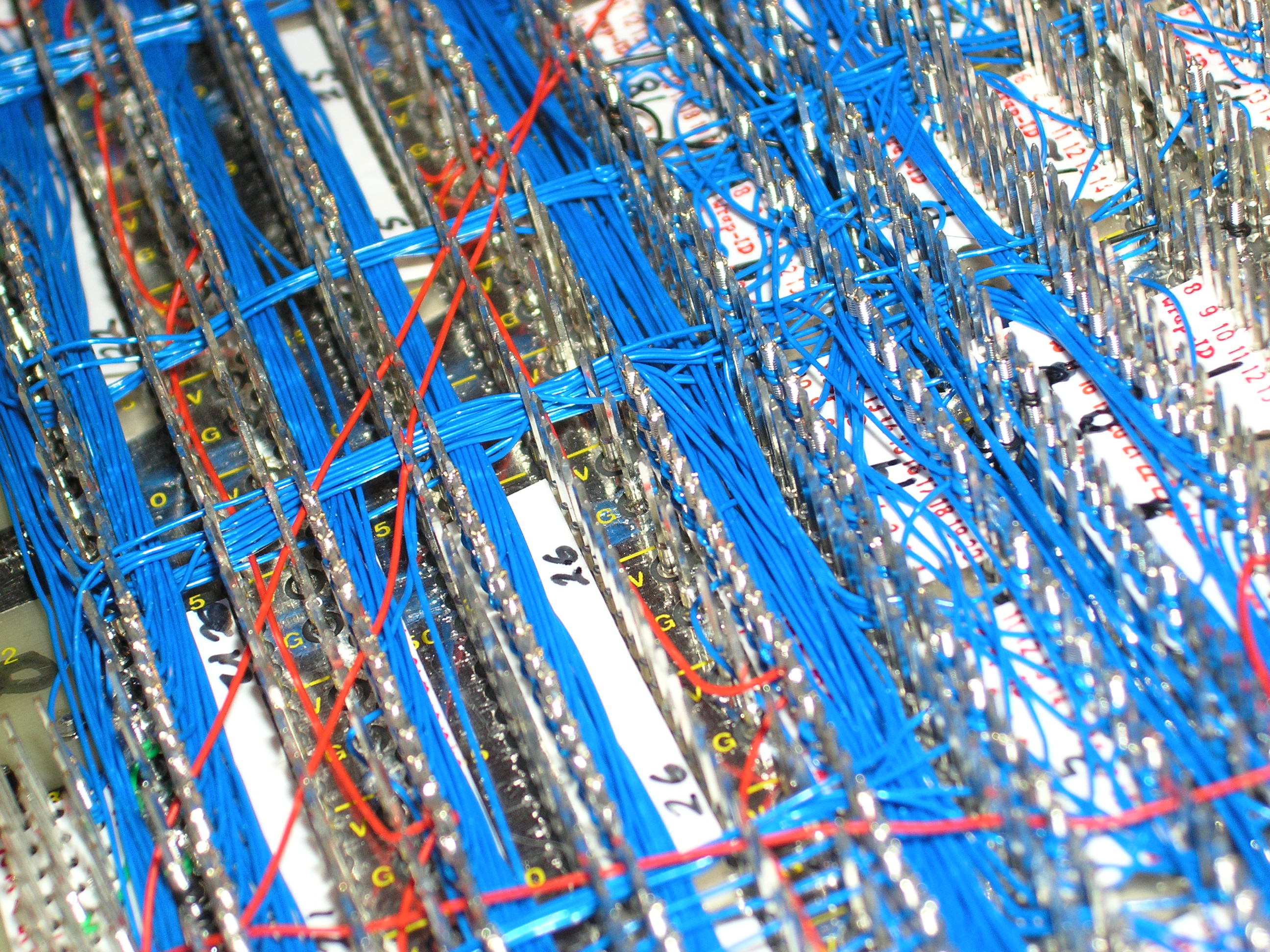
The memory card is very nearly complete. All of the signal wires are in. What's left is wiring up power/ground for each device and then soldering in the bypass capacitors on the component side. Should be able to finish in one more session. Note that I'm trying out my strategy for avoiding cross-talk on the important lines. Any wire connected to an edge-sensitive input uses red wire. All normal signal lines are blue. Ground is black and Vcc is green. The blue lines are constrained to follow the layout grid, unless the destination device is adjacent. This results in some fairly dense wire bundles, which I understand can lead to crosstalk. My assumption is that crosstalk is okay for level-senstive lines, because there will be enough time for the noise to settle. The red lines avoid the layout grid and bundles, making crosstalk less likely for the important edge-sensitive inputs. Of course, I am a software guy and don't really know what I'm talking about. But, it sounds good to me. Close-up photos of the wire wrap continue to amuse me. Here's another:
1/30/2004Very fast progress. Wrapping the SRAM portion of the memory card has gone quickly - lots of similar wires and easy to get into a good rythm. Here's where I am:
However, it's starting to slow down dramatically as I have to spend more time now with long wires and routing difficulties. The SRAM is basically done (just lacking power/ground). Next up is the page table circuitry, which is considerably more complex. Still projecting at least a week or two before I can start testing. 1/27/2004Did board prep (adding additional power/ground lines & capacitors) and then came up with a preliminary floor plan for chip placement. While doing this, I realized I was mistaken about the number of pins across the board - it is 81, not 80. This enabled me to modify the basic layout to give a pin space on either end, providing I reduced the center 16-pin slot to 14 pins. So, my standard layout will be: .10..10..10..7..10..10..10. Of course, when dealing with large chips, this changes a bit. I also went ahead and placed wire-wrap ID tags on the board (which was a bit of a pain because I had to construct some of them by cutting. I wanted to have the IDs down so I could sit and visualize the major wire routing before I start. The layout was largely driven by the needs of the A-bus, which touches about half of the chips on this board. Note that in the picture below, the diagram is the component side, and the board is wire-side up.
1/26/2004Need to think about this one for a bit before I start building. The card will be dominated by the SRAM, in 8 32-pin wide packages. The card also contains the page table logic, along with the page table fast sram (in two narrow 28-pin packages). For wire-wrap ID's, I'll cut down some 40-pin labels. I'll slice them down the middle, align and snip off the extra numbers. The first big effort will be deciding on chip layout. I previously decided to use a basic floorplan based on slots for 20-pin packages. There would be 7 slots for 20-pin packages, and a 16-pin slot in the middle. On the ends, there would be no free pins, but between all other packages there will be two free pins: 10..10..10..8..10..10..10 I'd originally thought I'd just burn two slots for each of the big chips (4-slots for wide chips - because they span two rows). However, this seems pretty silly for this card. The purpose of the orderly slots is to give me good vertical channels for running wires. Perhaps I can still do that by having a section of the board in my new layout, and another section of the board tailored for the 32-pin package. I also want to be very aware of the bus wires, and how they are going to route to the SRAM, page table and bus. I didn't do as well as I could have on the front panel logic card, so this will be a good chance to improve. |