|
|
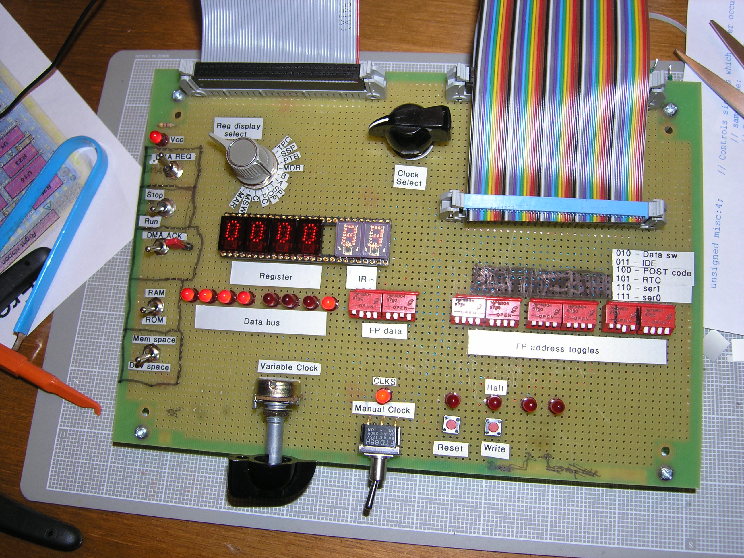
Temporary Front Panel Assembly ConstructionThe final front panel of Magic-1 is going to be fairly elaborate with lots of blinky lights and switches. For reasons including lack of desk space and the fact that I haven't yet finalized on my enclosure, I've decided to proceed with construction using a throw-away front panel LED/switch assembly. It won't include everything the real front panel will have, but will include what I need to test the system as I go. 4/8/2004Added support for register display, as well as displaying the current opcode. The register display is untested - need to have the alu/register card in place for that, but the opcode display seems to work just fine.
4/6/2004Decided to go ahead and add the register view function on the temporary card. This involves a rotary switch to select any of the registers which are capable of driving the L bus (which is just about all of them). When the clock is stopped, the switch takes effect immediately and the register is displayed. When the machine is running, a latch on the front panel control card grabs the most recent copy of the register selected by the switch (when the register is driving the L bus). To make this nicer, the HALT microcode consists of a loop which sequentially dumps each of the registers in turn onto the L bus - this way I can view everything easily from HALT. In the real front panel, the display will use LEDs. For the temporary front panel, I'll go ahead and use HP hex displays. While I'm at it, I'll also put in some hex displays to show the current instruction (i.e. - contents of the InstructionRegister (IR)). I want to have this capability before I begin bringup. Hope to start on it tommorow evening. 2/25/2004I may fiddle with this a bit, but it's pretty much done:
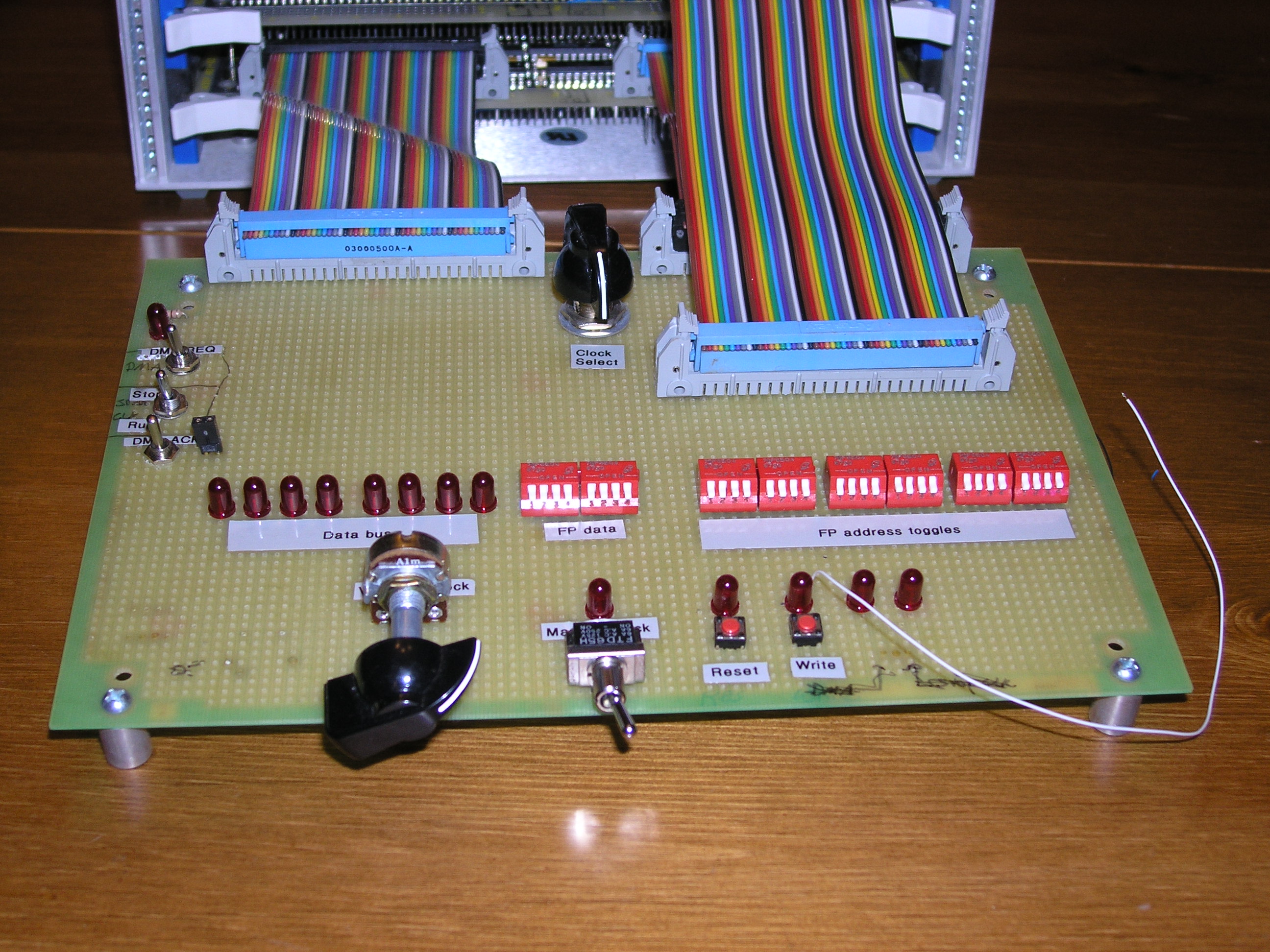
2/24/2004Lots of enhancements to the temporary front panel - and I think I probably won't do much more. By the time I need more front panel capabilities, I should be ready to start working on the real one. Today, I added the ribbon for the device card, and dip switches to mimic the real toggles for data and address lines. Here's what it looks like now:
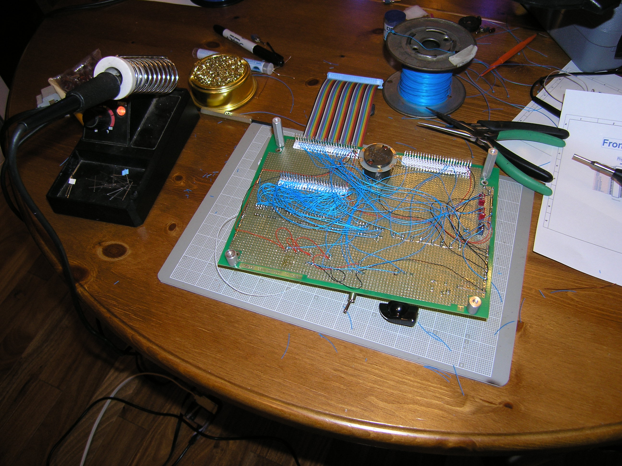
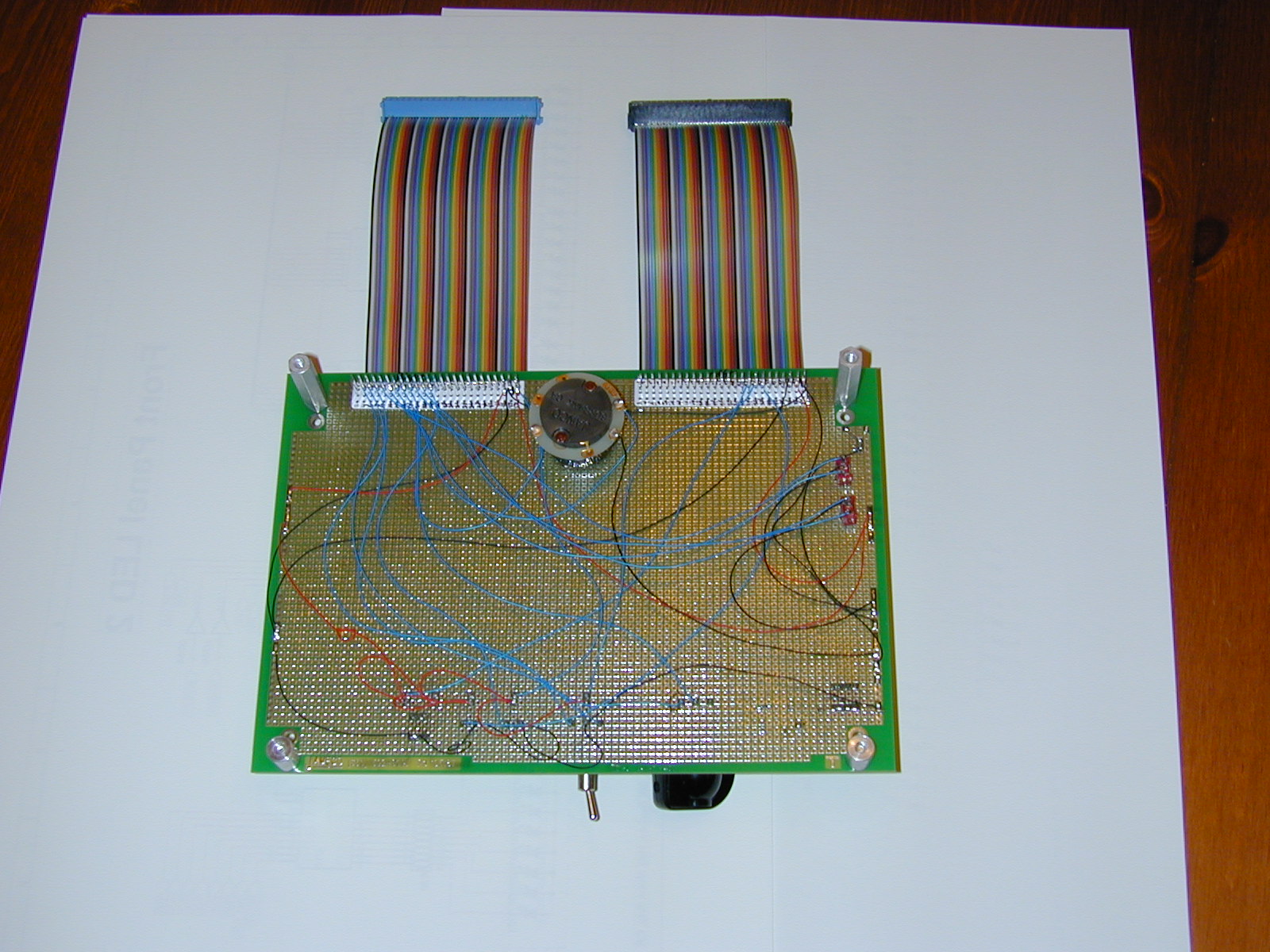
I still have a few toggle switches to add (for selecting between device and sram address spaces, and for selecting between ROM and RAM in the low 16K bytes of physical device address space. After that, I'll start testing. I was quite a bit more sloppy in the construction here - and am really tired of this card. Hope I don't have to much more work into it. Here's the gross backside:
1/18/2004
Included here are the necessary switches to test the clock generation logic: a 1M ohm pot (front), manual clock toggle (front center), small push buttons for reset and front panel write (to right of manual clock toggle), toggles for stop clock and DMA request (upper left) and a rotary switch for clock source select (top center). The DIP switches are currently usused.
|