|
|
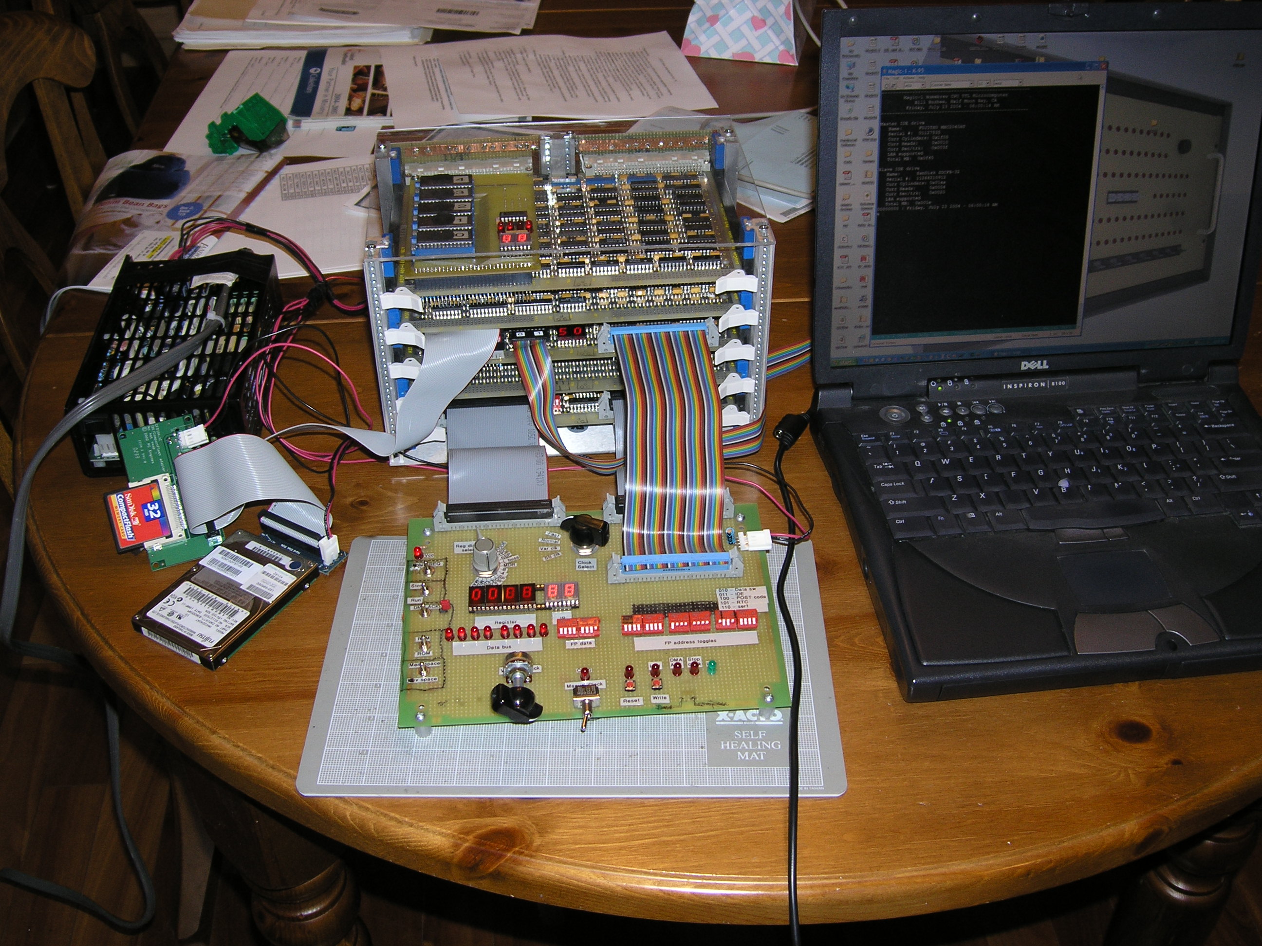
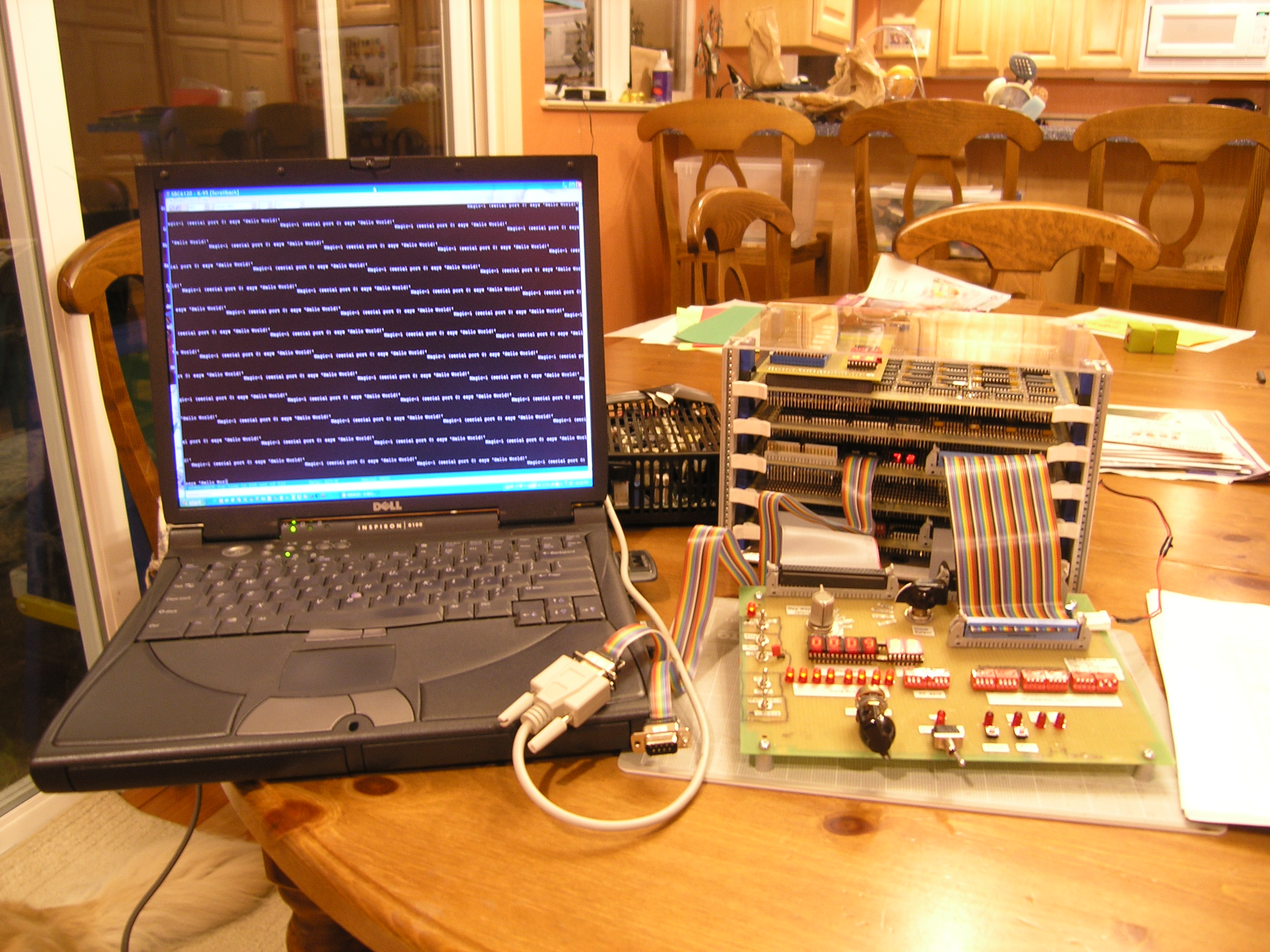
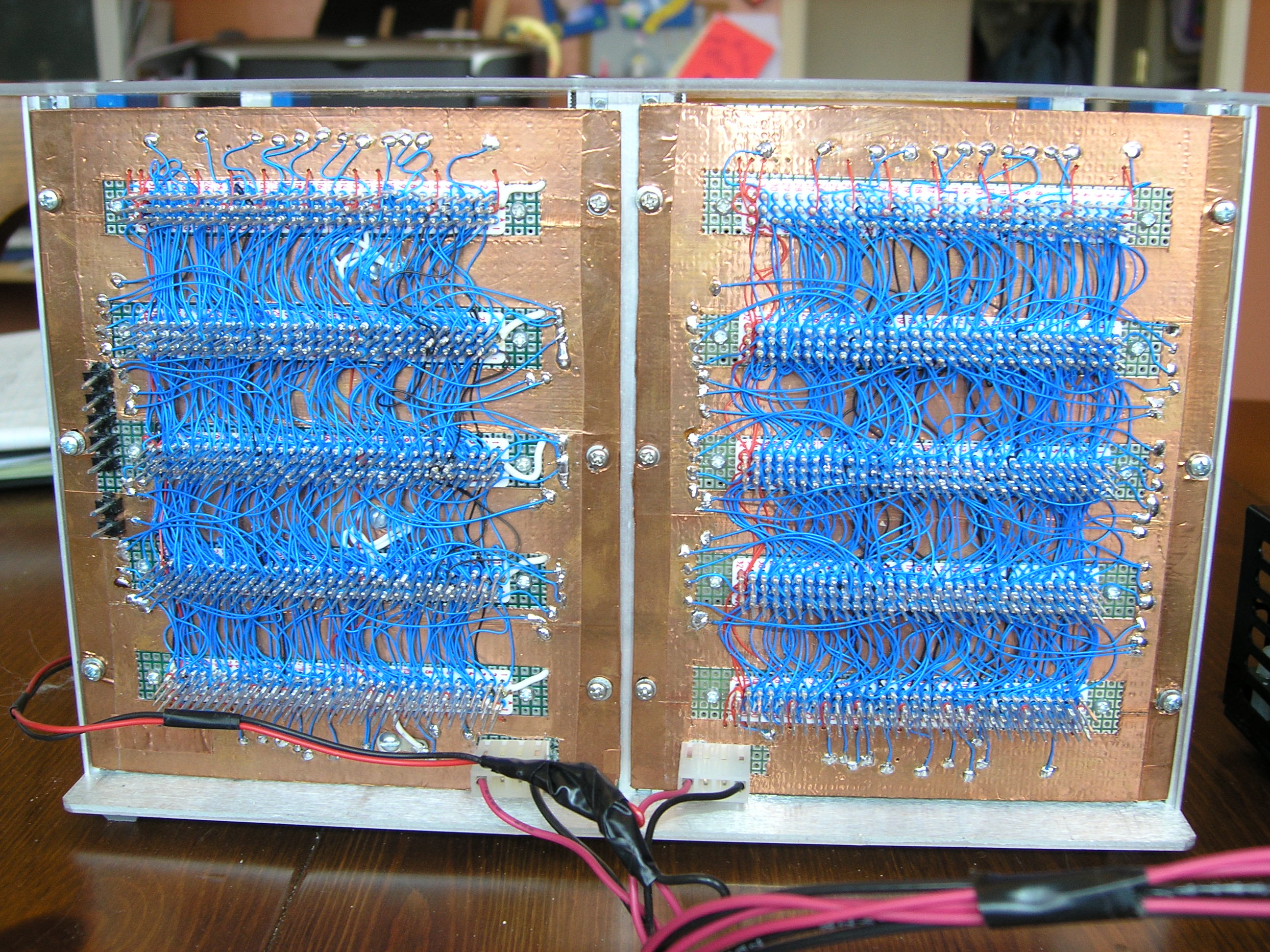
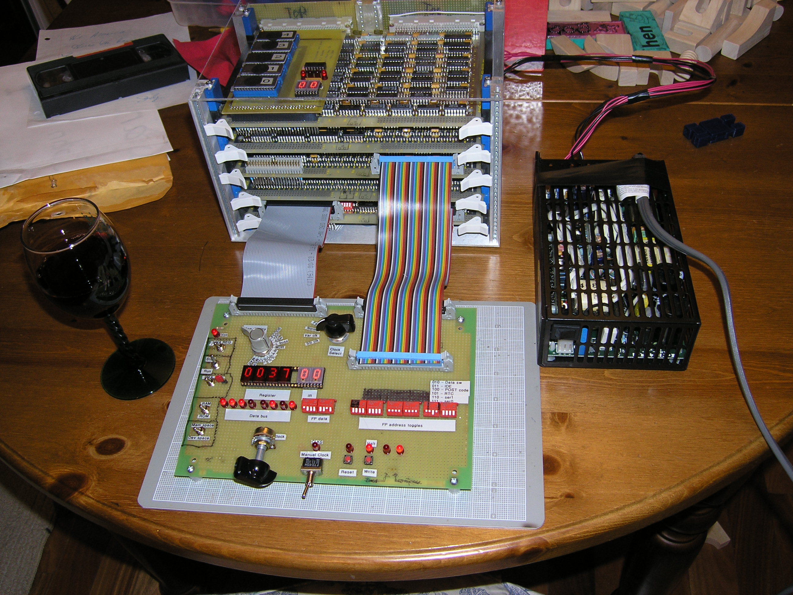
Completed - 7/23/20047/23/2004Everything checks out - my validation test suites and stress tests work. All bios functions work: IDE drive discovery, real-time clock time keeping and heartbeat timer interrupt, both serial ports reading and writing, the system clock slowdown circuit to access slow devices, the POST code displays - everything looks good. I had the machine run all night at 3.68 Mhz with a test that read input from my laptop via serial port 0, then printed out the current heartbeat timer interrupt count, time of day and echo the input line. I kept it running by using a butter knife to hold down the enter key on my laptop to blast the machine with empty lines, so M1 would echo everything as fast it possible at 9600 baud. All the while, it was programmatically dropping and raising the system clock speed and handling 64 timer interrupts a second(over 2 million by morning). All went well. So, I declare the bring-up of the basic electronics complete. Next up: software bring-up and buliding of the front panel and enclosure.
7/14/2004Haven't had time for any additional testing, but I am feeling a bit less convinced that I had a fan-out problem. Looking at the data sheets and the drive current required for F parts vs. LS parts, my 74LS244 bus driver should have been able to drive all of the consumers of CKLS - not by a lot, but it should have worked. One caveat, though - this signal was being run through a 47 Ohm resister for termination. I don't know how or if that would affect fanout. I've only run that one test, which failed when using a 74LS244 but passed with a 74F244. Puzzling. One other area to look at: the 74x244 CLKS driver is on the front panel card. The front panel card connects to the front panel assembly via a couple of ribbon cables. The front panel assembly draws a lot of power - enough that I give it its own power feed. Before I did that, it (and the front panel logic card) would show a significant voltage drop relative to the other cards. A while back the special power socket for the front panel assembly took a little damage when I assembled the machine. Perhaps it is connecting intermittently - if so, that could cause a power supply issue with the clock generating logic. I'll check that out as well (probably this Sunday). 7/12/2004I probably shouldn't say this out loud, but I think the basic hardware is complete. Have more testing to do, but I think I found the problem that's been plaguing me for weeks. I've had a bit of a rough time with the project lately. The problem with flying off into the weeds was *not* just an EPROM problem as I had hoped. I burned the same test program into several EPROMS and got consistent (but not exactly consistent) failures. Last Saturday was my big debugging day. I had some earlier sessions with the logic analyzer that gave very strange results, but I wasn't able those times to attach probes to what I believed were the key signals. On Saturday, I spent a lot of time setting up the logic analyzer to probe some hard-to-reach pins that I was convinced would show me the smoking gun. Extremely frustrating day: I couldn't get the analyzer to trigger properly. I redid the setup several time, checked grounds over and over again and then finally had the bright idea to run the self-test on the logic analyzer to make sure it was working properly. It wasn't. The self-test failed. So, my eBay special logic analyzer was broken and I had run out of ideas. The basic symptom that on some tests, I would fly off into the weeds when running over 1 Mhz or so. However, for other tests (including my validation suite) things would work just fine out to 3.68 Mhz. The problem arose after my rework for signal handling and the addition of a circuit to programmatically drop the clock speed in half to support slow devices. I'd spent hours and hours beeping out the reworked cards looking for wiring mistakes, examining the wiring with a magnifying glass to looks for loose bits of wire, double and triple-checking grounds and searching for bent pins. No luck at all. On my commute home from work today, though, a new possibility occured to me. Perhaps I had introduced a fan-out violation. During the design and construction, I had been very careful to calculate fanout and ensure I was well within margain. However, it dawned on me that when I had done those calculations, I was assuming that I was mostly consistently using TTL devices from within the same family. My recent rework involved replacing several LS devices with F ones to tighten up some signal windows. Those devices were driven by the primary system clock, CLKS. CLKS is generated on the front panel card via an LS part. Perhaps I was now exceeding its drive capacity? Tonight I replaced that LS part with a higher-power F device, and a test that used to consistently fail is now passing. There is much testing yet to do, and several times now I've believed to have solved the problem only to see it come back. However, this time it seems to make sense to me. I won't be able to properly test everything for a few days. But I'm cautiously optimistic. If that was the problem, I can declare the basic hardware complete. The signal handling looks good, and the circuit to drop the clock speed in half seems solid. 7/4/2004Wasted a few days tracking down what I hope wasn't a real problem. Last week I burned a new version of the bios test into one of my EPROMs. This particular test ran through all of my bios functions, including IDE drive discovery while fielding 64 timer interrupts per second. It failed. Things seemed to work okay at slow variable clock speed, and ran most of the time at < 1 Mhz, but immediately flew off into the weeds at 2.4 Mhz. I spent several sessions looking for bent pins, unseated chips or other mechanical failures. No luck. On two evenings I probed with the logic analyzer, and the results were very strange - couldn't come up with a hypothesis that made much sense. To add to the wierdness, my validation suite run and passed just fine. I even beefed up the decoupling capacitors on the control and alu/register boards (something that I'd been meaning to do anyway). No change. Finally, I thought I'd better rule out a bad EPROM. So, I burned the same test program into a different chip. Now, everything seems to work - even at 3.68 Mhz. I've been running the test since yesterday evening, and it's handled more than 3 million interrupts. Next up, I'll try to verify that the first EPROM was in fact bad - and see what happens with some of my other ones. In other news, I discovered that my guestbook for this site had been hacked. I ended up having to completely remove it. 6/30/2004Added the microcode NOP in "copy msw,a", and everything seems to work just fine now. I also went ahead and did the logic cleanup on the control board, freeing 3 or 4 gates. Updated and uploaded the schematics. Getting very close to calling hardware bring-up complete. All that's left is wiring up the slow-clock flip-flop and rewriting the fault and return from interrupt code to deal with saving and restoring in system space. Oh, also need to burn a set of real bi-polar proms to make sure I've got those wired up correctly. I want to put that off as late as possible, since they can only be burned once. 6/29/2004Found the problem. It was in interrupt handling issue, but had nothing to do with multiple interrupts pending. Instead, there was a problem if any was pending when interrupts were enabled. The interrupt enable bit of the MSW would transition from off to on on the rising edge of CLK_S, and if that microinstruction also represented an instruction boundary, the pending interrupt would be recognized immediately. However, we would have already clocked in a no-interrupt fault code. So, we'd fly off into the weeds after trying to use the illegal interrupt vector 0 again. Anyway, I believe there is a trivial fix for this problem - just adding a microinstruction NOP between the transition of the interrupt enable bit and the ending microinstruction. There are two places where the E bit can transtion from off to on, "copy msw,a" and "reti". The problem only shows up on the copy. It's late, I'll make the changes tommorow. 6/28/2004The interrupt handling is looking good. I modified the looping validation suite to turn on the real-time clock's heartbeat interrupt. It ran just fine for an hour. I then hooked up my logic pulser to drive interrupts at 100 Hz on IRQ0 and IRQ4. No problems at all - the test loops and handles 264 interrupts a second while passing tests. I'll leave it on overnight, but I'm thinking now that my problems yesterday had nothing to do with multiple interrupts. A real possibility is that my bios test is flying off into the weeds because of a C compiler error. Since I last ran the bios tests, I've done a lot of changes, so perhaps I introduced a bug. If that's the problem, it should be fairly easy to find and correct. I did some work around register usage around procedure calls, so I could easy have screwed up register spills around call sites. 6/27/2004Making progress. I ran a heartbeat interrupt timer test and it worked great. I programmed the real-time clock to send an interrupt 64 times a second, and then had an interrupt handler that incremented a 32-bit tick counter and returned. I let this run for more than 4 hours, and the tick count matched what I expected. There are still some problems, though. When I turned on all bios features - the real-time clock, serial ports and IDE drive discovery, I flew off into the weeds near the point where I enabled interrupts following IDE drive discovery. I think the problem happened when I had multiple pending interrupts (from the RTC and the IDE interface), but I'm not sure. The weeds I'm flying into appear to be related to top of stack. I don't have time to look further tonight, and may not for a few days. My validation suite runs great, but the current version does so with interrupts disabled. I'll see what I can do to have a version that loops with interrupts active. Then, I'll have the RTC pound it continually with timer interrupts. If I have a problem with correctly fielding interrupts only between instructions, this would catch it (eventually). To get that to work, I'll have to make sure I always have a valid SP, or disable/renable interrupts around tests that use a bogus SP. 6/26/2004 [update]Yup - that was it. I spent some more time with the logic analyzer and discovered (to my horror) that the time lag between signals which clock registers and the one that clocks the MSW condition code bits was somewhere in the vicinity of 40 nanoseconds (my analyzer only has a 10 nanosecond resolution). The worst part of this, is I remember now that I had earlier calculated this particular path and did seemingly odd CLK_M wiring specifically to narrow this window. When reworking for interrupts, I had forgotten all about this and when I encountered the strange CLK_M wiring path, I "simplified" it. And broke everything in the process. On the bright side, what I have now is much tighter. Besides restoring my odd CLK_M wiring, I put a few more F parts in the generation path for L_MSW. My clocking signal window is now down to around 10 nanoseconds. That should be narrow enough - it gives me 20+ nanoseconds to spare for Z-bit generation. I've been working on this problem long enough now that I don't exactly remember where I was with the interrupt handling rework. I think that I'm ready to start testing the heartbeat timer handler (from the real-time clock). However, I know that I didn't complete the wiring. The new scheme will allow some additional gates to be freed, and I can collapse a couple of two-input gates into a single three-input one (which I have free). These changes, though, won't change the functionality - which I believe is complete. Once things are working, I'll go back and clean up these unneeded gates. Or not. Oh, just to remind myself - I need to rewrite the interrupt handling microcode to ensure that the mode bit is changed to supervisor mode before saving register state onto the kernel stack. I had originally been relying on the IN_TRAP bit to allow hardware to make sure the right memory space was used, however I neglected to assign a backplane signal for it. It's generated on the control card, but would have been consumed on the memory card's page table logic. However, when looking it over, I believe I can do away with this bit if I get a little tricky in my register save/restore order in the microcode. 6/26/2004OK, the world is still broken, but I believe I am getting close to understanding the problem. First, the issue I had the other day with the logic analyzer's glitch detection turned out to be the usual problem: pilot error. When hooking up the pod, I grounded the wrong lead. No wonder everything was screwy - the pod wasn't grounded. With that fixed, I showed no clock or L_MSW glitches. What I did see, however, was a likely timing problem. One of the worst aspects of my design is my simple clock scheme. I understand much better now why most microprocessors have complex, multi-phase clocks. Mine is essentially single-phase (except for a few places). I rely on lots of things happening "at the same time". Of course, nothing here happens at exactly the same time, given propogation and gate delays. In a nutshell, here is what I think is happening in the case in which a=0, a=a+8 and Zero bit is set on the result:
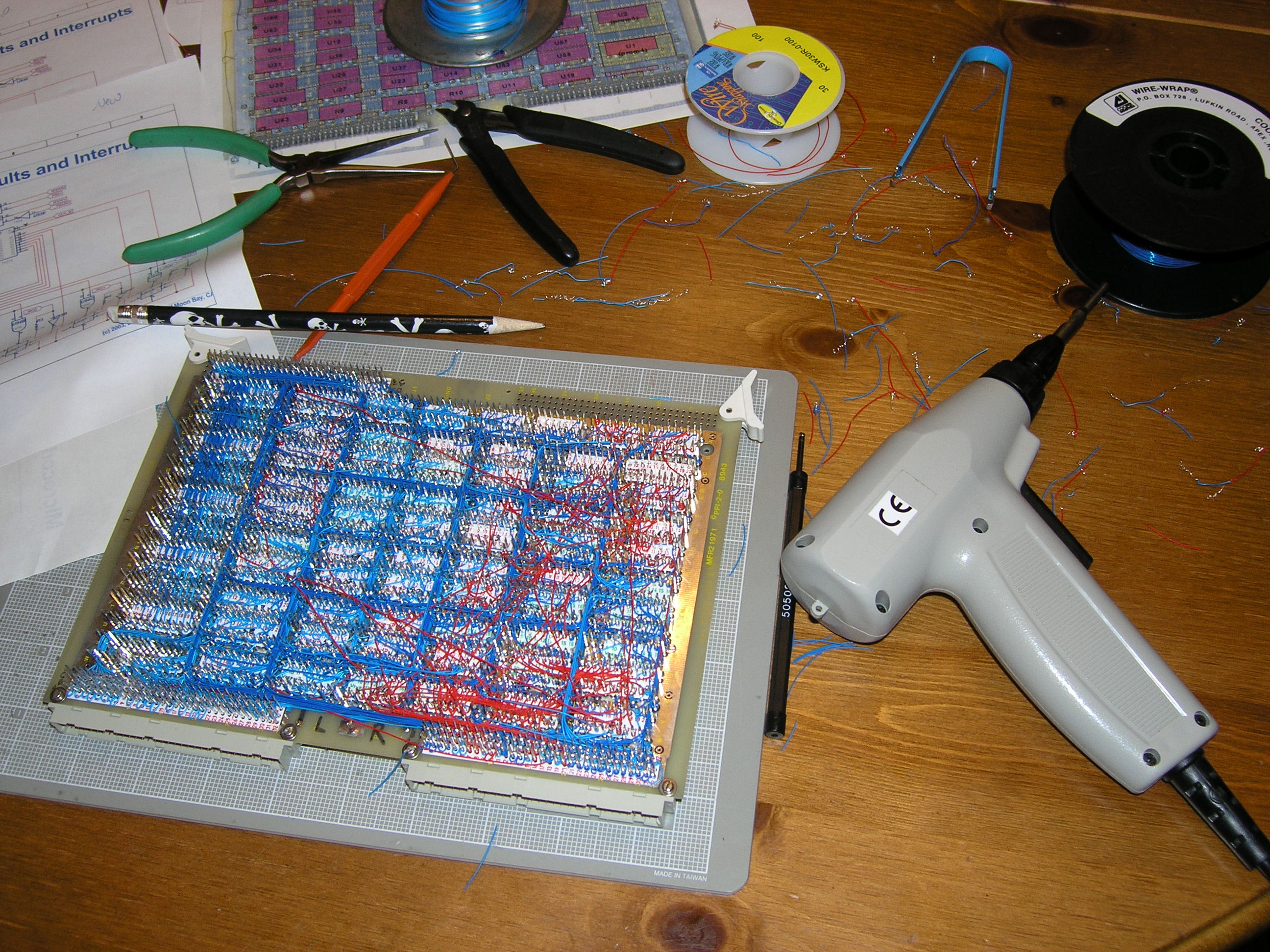
Or at least given what I saw on the logic analyzer, that scenario seems possible. It also makes sense when I think about the wiring rework I did on the control board. One of my changes involved CLK_M, and had the effect of adding a bus-driver gate delay to it. It is conceivable that that delay was enough to open my critical window too wide. It also makes sense in that differing clock speeds had little affect on the problem. The speed of the clock is irrelevent here - it's the propogation delay window that matters. As a quick test, I swapped out a 74LS00 nand package for a high-speed 74F00 one along the CLK_M generation path. Doing this made my simple looping test pass. However, it still failed the validation suite (at a different place - this time a subtract). I am hopeful, though, that it is the same problem - just minute timing differences. What I need to do, I believe, is ensure that the window stretching between the first of my clocking signals to the last of them is shorter than the time it takes for anything to change. First step is to change my CLK_M rework to ensure that time-critical consumers of CLK_M get it as fast as possible. Next, I'll look at swapping LS and F parts to try to even things out. 6/23/2004Having a bit of a bad spell with the project. After the rework, I failed my validation suite. Over the last few days I've been narrowing the problem until I had a tiny test program which reads the front panel dbus switches into register A, adds 0 to register A and then loops back if the result of the addition is non-zero (i.e. Z-bit == 0). If the Z bit is set, control falls into a HALT instruction. Here's the weirdness: if we add (0x08+0) or (0x80+0), the Z bit is occasionally set (but not always), when it shouldn't be. The result of the addition is correct - it appears to be the computation of the Z bit that fails. Further, it appears to be timining related. Depending on the clock speed, one of 0x08 or 0x80 tends to fail more often. Now, to compound the weirdness, all of this is happening on the ALU/Register board, which had no changes in the rework. With a problem so well defined with a small test program, I figured this would be very easy to find and fix. But no - it's been driving me nuts. I've carefully examined all of the wiring in the Z-bit computation circuit, and have even added piggy-back wiring on the theory that I might have a wire that was snapped inside the insulation, but still conducting intermittenly. Also added additional power/ground on U21, which is key to the circuit for the 0x80 and 0x08 bits. No go. After this, I thought that perhaps the Z bit was being computed properly, but maybe a glitch on L_MSW, the signal which clocks new values into the Z-bit flip-flop, was stuffing in the incorrect value after the good value had been set. So, tonight I pulled out the logic analyzer. I advertises a "glitch detection" mode, which I had never used before. I hooked it up in glitch mode, and told it to stop on a glitch on CLK_S, CLK_M or L_MSW. I started the trace, and got an immediate glitch detect. In fact, after fiddling with things for awhile, it seems I had nothing but glitches - glitches on every signal I tried. This didn't seem right, so I tried to narrow the problem further by powering up only the board with the clock generation circuitry. I did it outside of the card cage, powered by my bench supply. In this configuration, I believed I should be a very clean CLK_S signal. However, my logic analyzer kept on reporting glitch detection even in that situation. All I had was a oscilator going through mux. Glitch detect fired on both the input and output of the mux. This just can't be right. I then pulled out the oscilloscope, and the CLK_S signal looked great - nice, clean and crisp. At this point, I think either my logic analyzer if flakey, or I set it up incorrectly for glitch detection. Ugh. Think I'd better sleep on it. I'm not entirely sure which direction to probe at this point. 6/17/2004Finished the rework wiring, but all is not well. It was late, but I tried some quick runs to see if things had improved. I pass the old validation suite occasionally at slow variable clock speed, but not at normal speed - and my interrupt test quickly flies off into the weeds. Probably damaged a wire or two during the rework. First thing I'll do is very carefully examine the board to see if there's a wire fragment shorting something, followed by beeping out all of the connections. 6/16/2004Began the rework to attempt to fix the interrupt handling. It's slow-going and difficult, but I can really appreciate the reason that you do a wire-wrap chain wrapping every other connection first. That way, at most you have to remove 3 wires to replace one. If you went a->b->c->d...etc., you could have to undo the entire chain for a repair. Anyway, I'm about half done. Here's the aftermath of tonight's session:
6/10/2004My 4-year-old son woke up at 3 a.m. this morning with a bad dream. While trying to get myself back to sleep after getting him back to sleep, it occurred to me why I was flying off into the weeds after a few seconds with the heartbeat timer on. The problem is, as Dave Conroy pointed out, the lack of synchronization between the incoming interrupts and the rest of the control circuitry. The fault code register (FCODE) is clocked at the rising edge of CLK_M on each instruction boundary and detected faulting condition. However, there is no synchronization between this action and the arrival of an asynchronous signals which will affect the priority encoder. The "fly off into the weeds" case happens if the timer interrupt arrives just after FCODE was clocked (and stored a 0 representing no interrupt), but just before the output of the priority encoder was used to vector control to the trap handling code. The changed encoder would have sent control to microcode address 0x101, which would then branch to the common interrupt/fault code. That code would then use the contents of FCODE to load the address of the trap/interrupt handler. In our error case, it would load the value at interrupt vector 0, rather than 1. Interrupt vector 0 is an "impossible" vector, and rather than having the address of a handler instead contains the short branch at physcial adress 0x0000 that branches around the interrupt vector. Nevertheless, those bytes were loaded and branched to - sending us into the weeds. I believe my proposed redesign to add a 74273 register between the interrupt flip-flops and the priority encoder, as well as moving the clocking of FCODE to the rising edge of CLK_S rather than CLK_M should do the trick here. I review this all again tommorow, and if it still seems to make sense I'll make the changes. 6/9/2004I've spent quite a bit of time staring at my interrupt and microcode sequencer schematics, and found several areas that seem suspect. In particular, there is timing nastiness dealing with holding the current value of the encoder stable across the entire high period of the system clock, and with the way the IN_TRAP and IRQ flip-flops are being reset. When I started this project, I was a little puzzled why all the designs I looked had more than one clock - usually overlapped or phase-shifted. Now I think I understand. With my simple clock scheme I am relying on the order in which signals arrive to avoid problems. For example, when a faulting condition is detected, I have a FAULT_PENDING signal active. One of its major functions is to suppress edge-senstive clock signals to avoid clocking in bad data to registers. The potential problem arises if, on the falling edge of the system clock, the FAULT_PENDING signal is deasserted ahead of CLK_S. In that case, a nasty glitch would occur and cause register values to change. I believe I've ensured that in all of these cases CLK_S will arrive before the deassertion of FAULT_PENDING, but it I had a more sophisticated clocking scheme I could ensure this, rather than rely on propogation delays. Anyway, I believe I have some changes that will significantly simplify the interrupt handling. It mostly involves moving all of the important actions to happen on the rising edge of CLK_S (right now, half happen on rising edge, and half happens on falling edge). As an added bonus, the fixes will result in fewer gates. I will completely elminate the problem flip-flop, as well as several and/nand gates. This should take care of Dave C's issue with my flip-flop clocking. The other issue - synchronizing the asynchronous interrupt requests - I believe I can handle by adding a 74273 register between the six IRQ flip-flops and the lower priority encoder. I would clock this register on the falling edge of CLK_S, where it would take a snapshot of the current interrupt request state. This state would be presented to the priority encoder and would be held stable for the entire clock cycle, ensuring that nothing odd happened at the critical point of the CLK_S rising edge. As far as space on the board, the elimination of the flip-flop means freeing up an entire chip slot, which I can then use for the 74273. That will still leave me with one spare slot. Although the changes are relatively few, it will be difficult. The interrupt/trap section of the board was one of the first I completed, which means the wires will largely all be found deep within tight bundles. There is a very good chance I'll cause some damage to unrelated wires during the rework. So, before I start I want to make extra sure that what I'm doing is the right thing. I think I'll review my proposed changes tommorow, and perhaps Friday as well before I actually start fiddling with wires. 6/8/2004Ran into some problems with interrupt handling. I knew I might have some exposure here - Dave Conroy pointed out a couple of problems earlier. One dealt with a flip-flop I'd put on the faults/interrupt sheet. Its purpose was to keep the "fault_pending" signal high across the entire high period of the system clock. I was clocking the flip-flop with the system clock, and also resetting it with the same system clock signal. What I hoped was a fix for this was to add a gate delay before the flip-flop clock input. That way the asynchronous clear should deassert a fewnanoseconds prior to the clocking edge from the system clock. I used a spare gate from U61 - a 74LS32 OR package. Maybe that helped, maybe not. Not sure how long the async clear must be deasserted before the clocking edge arrives. My problem symptoms showed up when I added an interrupt handler for M1's heartbeat timer. I programmed the real-time clock to interrupt at 64 Hz. The interrupt handler simply counts the ticks using a 32-bit counter. Here's what I'm seeing:
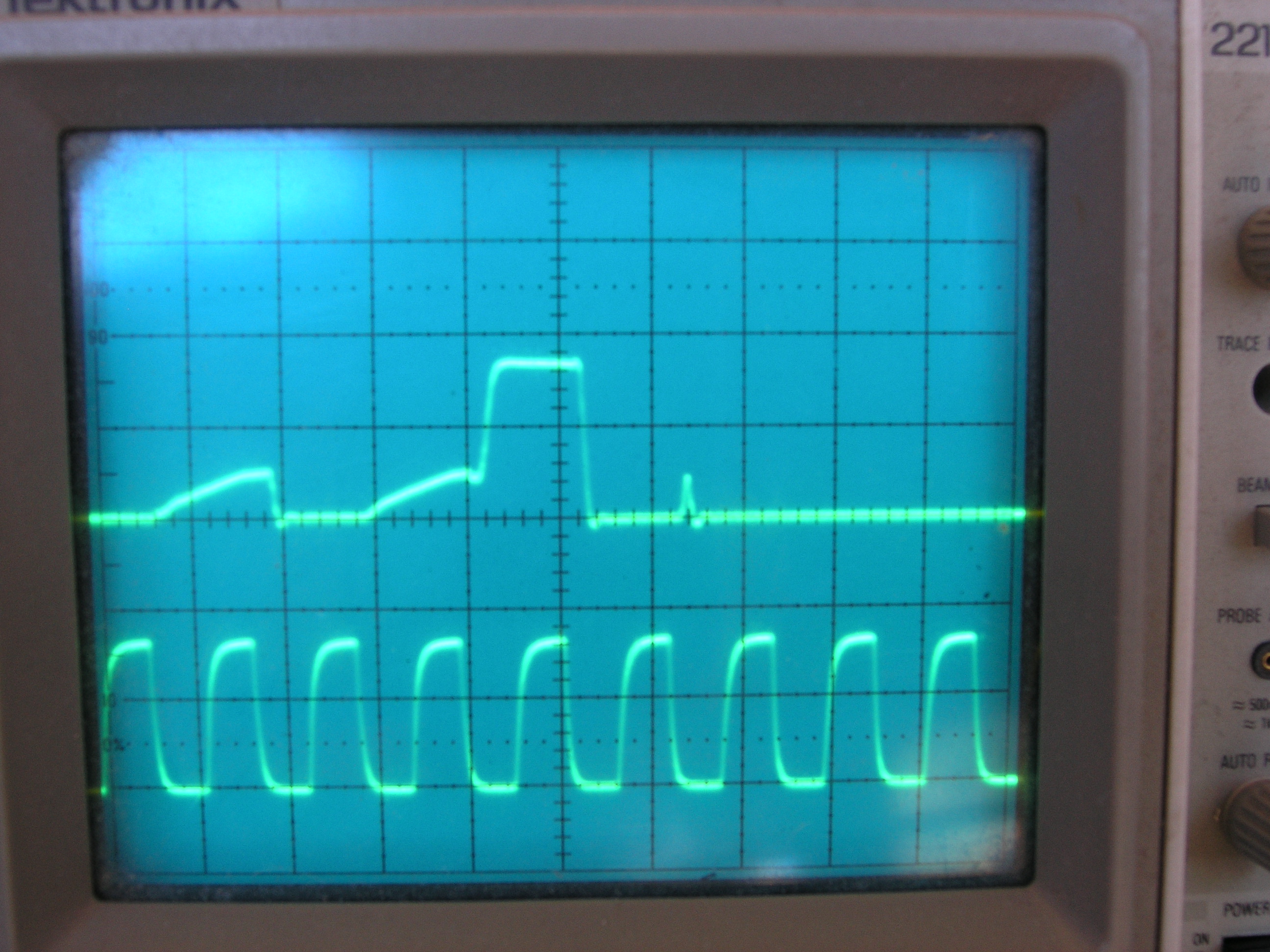
The other problem Dave mentioned had something to do with (from my faulty memory, now) a "syncronizer" for the flip-flops that recorded interrupt requests from IRQ0 through IRQ4 (all of this on the fault/interrupt schematic sheets of the hardware design). I don't understand this one, but apparently there's an issue with asynchronous signals that you need to have two flip-flops per signal in order to be reliable. Perhaps this is my problem? It's been long enough that I'm going to need to spend some time studying my design to remember exactly what it was I was trying to do. I fear significant redesign here, which would be bad because of the very high wire density on the control card, and the fact that I have only 1 free device slot (unless i canabalize the safety region I set aside for possible future replacement of the 20-pin .3 PROMs with 28-pin .6 EPROMs). 6/6/2004Finally got around to scoping out the data bus. I think everything's okay - what I saw seemed to match my expectations. I used some special microcode that transitioned between the LSB of the data bus floating, driven low and driven high. Here's a picture:
The botton trace is the system clock. The top trace is DBUS[7] (big-endian LSB). Starting with the clock cycle on the left, I interpret:
All of this matches what I expect from the microcode. It does get a little odd starting with slight blip. If I am correctly interpreting where this matches my microcode program, I expect the sequence starting at the blip to be:
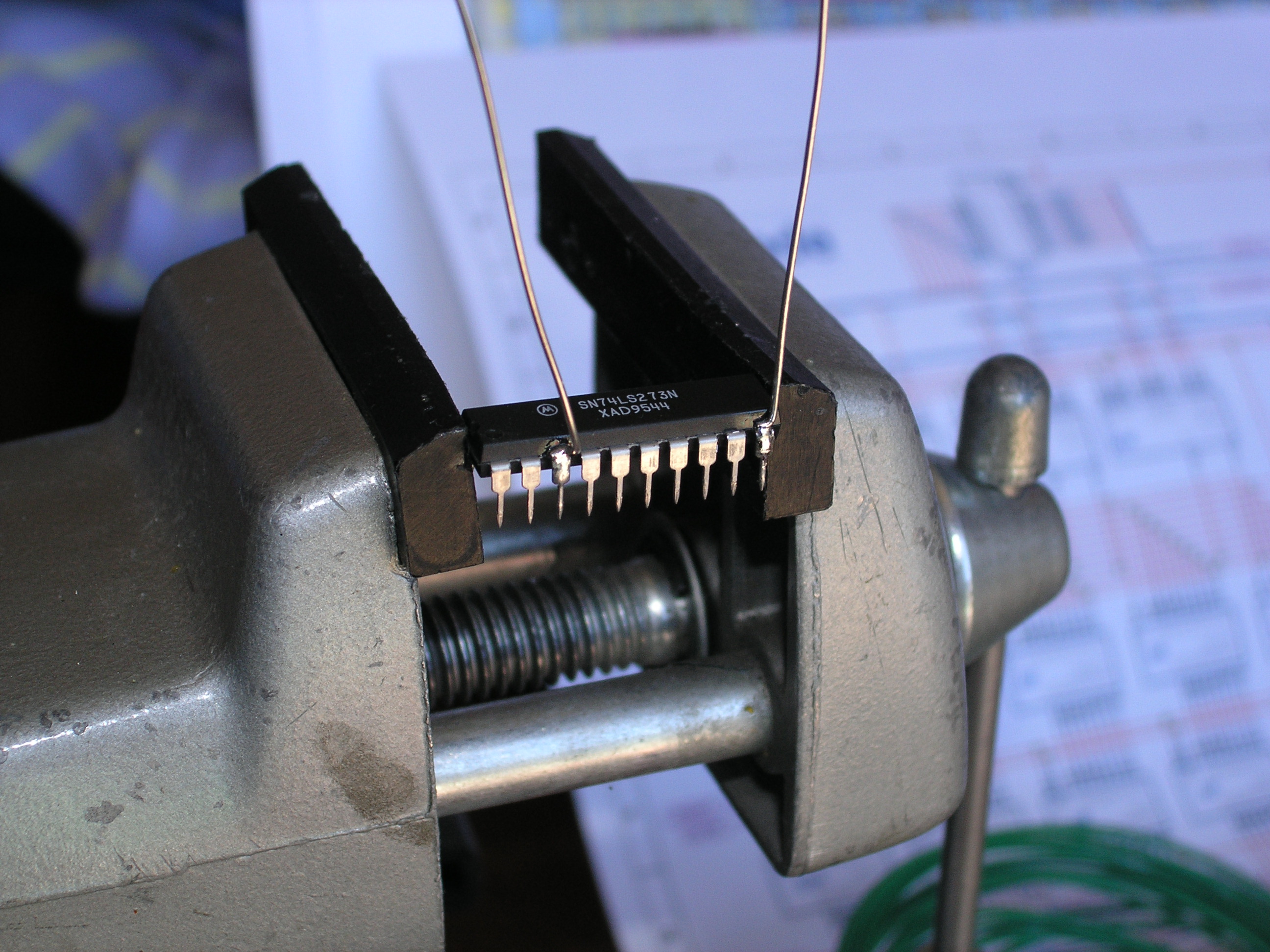
So, the oddity here is that I appear to have an undriven line doing a nice shallow rise in the left half of the trace, but doing a blip on the right side. Other than that, this all matches my expectations. Before closing this experiment out, a bit of methodology. To get clean signals I took Dave Conroy's advice and soldered some wires to the chip leads I wanted to probe:
I then wrapped these around the probes to give me as short leads a possible (trimming off the extra wire). It was also useful in that I didn't halt to try to hold a probe and look at the scope at the same time:
Unless I hear from someone with a different interpretation of my pictures, I think I'll consider this experiment concluded. The main issue was to double-check that I wasn't getting more than one device driving the bus at the same time. I think I'm okay on that score. Next up is to adding in the new ciruit to give the machine the ability to programmatically cut its clock speed in half in order to access slow devices. Once that's done and tested, I'll declare basic hardware bring-up complete (and move on to the software bring-up). Also, I got an email from John Doran the other day announcing a web page with more detail on his fantasic D16/M homebrew machine. Check it out. While looking over his instruction set, it occurred to me that it wouldn't be that difficult to retarget lcc for his machine. So I did. Only took a few hours, and other than some minor issues with generating references to frame local variables, the generated code isn't too bad. Sometime soon here I'll start a new page on this site for the software bring-up. At that time I'll post my lcc retargetings for both M-1 and D16/M. 5/30/2004Spending most time lately attending to the rest of my life, but have done quite a bit of work on the C compiler (lcc). What I did earlier was pretty reasonable for 16-bit ints and chars, but I hadn't put any significant time into 32-bit ints and floats. The code for them was really awful, and largely incorrect. So, I've been hacking on my lcc retargeting to get those in shape. Things are looking pretty good now. The code for 32-bit operations is still a little off, but good enough for my purposes. I'd expect 32-bit ints and floats to only have incidental use. My natural machine size calls for 16-bit ints - and the codegen for them looks good. Going into this process, I had 8 open opcodes. I now have 1. I added a set of instructions to improve generation of indexed addresses: sh0add r,r,r and sh1add r,r,r. If I had opcode space, I would have also added a sh2add r,r,r. Those are nice instructions - shift one operand left 0 or 1 places, and add to other operand. Besides generating indexed addresses, they are quite useful for building up inline multiplcations by small constants. For example, you could multiply register A by 10 as follows:
If I had sh2add, I could do a multiply by 10 in two instructdions. I don't have the opcode space to cover all register combinations. I could alias some of the sh0add's with register A targets to simple add.16 a,b and add.16 a,b. The difference is that my shxadds don't set flags, whereas normal adds do. I'll probably fiddle with this some, but the code generated for array accesses looks pretty nice now. My dilemma is that I really want to add some Forth primitive instructions. I suspect I'll do some more minor adjustments of the instruction set. Overall, the C compiler is looking good. I've been throwing hundreds of C files at it, and I haven't had any compiler aborts in a day or so. For the test input, I'm using the Minix sources. I do get quite a few errors and warnings, but that's to be expected given that I haven't seriously looked at which Makefile flags to set. My biggest software limitation now is my hacked up assembler and lack of a linker. I haven't touched the actual machine in a week, but hope to find some time tommorow to wire up the new slow clock circuit, as well as scope out the data bus. 5/22/2004Haven't yet had the chance to break out the oscilloscope & logic analyzer to do my (hopefully) last check of the data bus. Before I declare hardware bringup complete and move on to the software effort, I want to double-check to make sure I don't have any contention on the databus. Also, I've pretty much decided to abandon any further investigations of the odd UART behavior. I tried an 8250, and it behaved as I would have expected - the register values drove the dbus and held while using the front panel. Between that and the experiment with the 16550 isolated in the breadboard, I am inclined to write off the blinking out as a feature of that particular device. Also, I've been pounding on the uarts lately with the bios development, and they seem to work just fine. Speaking of the bios, it's getting pretty functional. I have entries to read and write characters and strings to and from both UARTS, real-time-clock access routines and a pretty full complement of IDE hard-drive support. I can initialize the drives, get drive info, set power-down behavior and read/write sectors. I've spent most of my time lately working on that code - mostly in getting the timeout and error handling behavior in shape. It's not completely polished, but works well enough for now. The bios is written completely in C, and I haven't run into any lcc retargeting problems for a while now. The biggest software stack issue at the moment is the assembler and the lack of runtime support routines for multiplication, division, floating point operations and general 32-bit integer manipulation. More discussion on the issues here when I finish hardware bringup and start the software bringup in earnest. The other hardware thing I've done is design a circuit for supporting slow devices. The real-time clock doesn't handle clock speeds much greater than 2.4 MHz, and the 8255 starts getting flakey around 3 MHz. What I did was add a couple of flip-flops and assorted glue logic to support switching to a half-speed clock on the fly. On reset, the machine will start off in half-speed mode. Storing a 1 to device 1 (0x000ffffff90) will switch back to the full-speed clock. Device drivers will be expected to manage this explicitly. It's a write-only bit, so the OS will have to track its current state with a shadow variable. The logic shows up on the ramrom and clock schematic sheets in the hardware design document. I also had to free up a line on the backplane, and ended up sacrificing the ground line at Left, B-2. Note that with this change the left and right backplanes are no longer identical with respect to power/ground usage. Anyway, before I wire this up, I want to wait a day and make sure it still looks reasonable. Oh, I also added a green LED to the temporary front panel for IDE drive activity. Now it really seems line a real computer - blinky disk activity. 5/20/2004Found the problem: a wire-wrap pin coming out of the backplane was bent just enough to short against its neighbor. The two shorted pins were L bus enables for the TPC and MDR, and so fought each other any time either was intended to drive the L bus. I'm now back to solid running of my validation suite in an endless loop at 3.68 MHz. Things also look better on the enclosure front. Found some much more reasonably priced enclosures from Bud and Hammond. Still hope I can find something surplus, but I haven't had any luck so far and the bent backplane pin is clear evidence that I need to put this thing in a solid enclosure and stop moving it in and out of the plastic bin. To further that goal, I'll be pushing towards getting the serial-port program loader written. 5/18/2004Couple of setbacks tonight. First, I requested a quote from a manufacturer of 6U instrument cases. I'd been warned to sit down before I reviewed the price list. Even so, I was shocked. Damn, expensive stuff. Think I'll keep looking in the surplus shops for a while longer. The second setback is a bit more ominous. I've been mucking around with device support for the last week or so, and have been running M-1 very slow to avoid problems with my slow device chips. I think I mostly was going at 250 KHz. Anyway, I decided to push the clock back up, and my device test programs started acting unreliable at even 500 KHz. That shouldn't happen until somewhere around 2 MHz. So, I dug out my validation test suite and found that I was failing at all speeds. I pulled the cards and looked for something obvious. Then, things got worse. Nothing runs now - the machine seems to pretty immediately lose its mind. When beeping out the machine before bring-up, I found a disturbing number of wires that were snapped inside of the insulation. I was afraid I'd have one go bad later, and I'm guessing that's what happened. I do way too much board pulling - my boot EPROM socket is only accessable when you pull a board, and I have to pull two boards to remove the temporary front panel in order to pack the machine up every night to clear the kitchen table. I'll bet all of that mechanical stress has caused something to break or short. On the bright side, I'd much rather have a complete failure (like it is now), than in intermittent one. I don't have time tonight, but I don't expect it will take too much time to find out why nothing is working at the moment. AFter it's running again, I really must do a serial port program loader in the bios so I don't have to pull cards as often, but rather just load test program via the UART. 5/17/2004Exploring the UART strangeness in which registers don't drive the bus lines high for more than a couple of seconds when accessing the UARTs via the front panel switches. I decided to try to isolate the situation, and wired up one of the UARTs on my old Heathkit breadboard. The UART behaved just as it did in M-1: the register output will only hold high values for a short time, then drop to low (note - low, not three-state). Here's what I did:
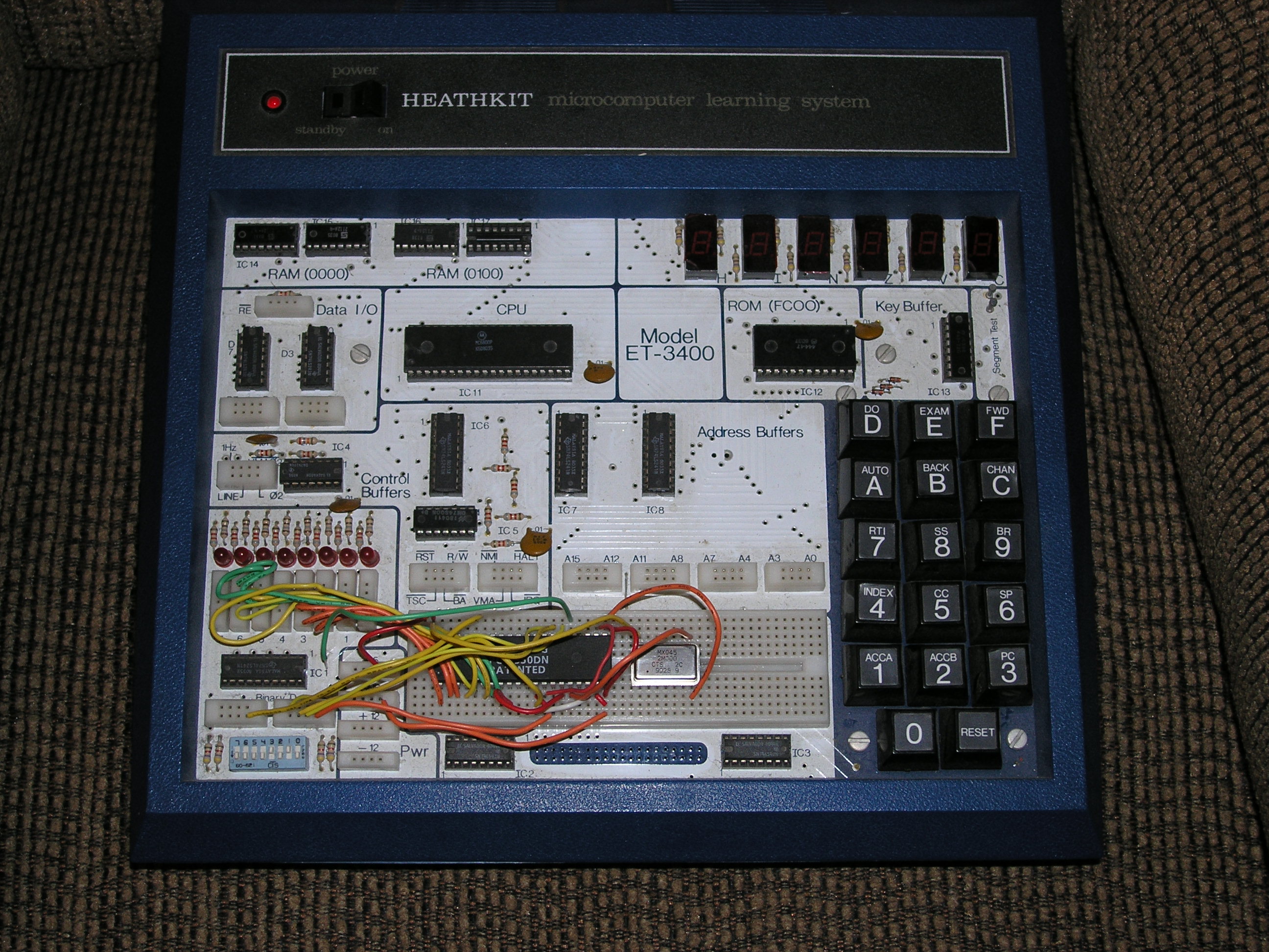
So, it could be that I'm consistently wiring this things up wrong, or that I've got a couple of damaged devices. The third possibility is that this is the way they are supposed to work. Just for kicks, I'm going to try a compatible, but different version of the UART, an 8250. 5/16/2004Exciting stuff on the enclosure front. Alistair Roe put together some fantastic concept models of what a completed Magic-1 might look like. Look here to see them. I was casually poking around for a surplus 6U enclosure, but now I'm quite anxious to find one. This machine is really going to look fantastic. And, it's running pretty well at the moment too. I was out of town on a business trip and didn't get too much done, but I was able to write some IDE drive access routines. After a hickup or two, it's now working well. I haven't tried doing sector read/write yet, but I'm pretty confident that will work. What is currently supported is that the bios does a reset of all IDE drives, and then searches for both the master and slave device. When it finds one, it intializes it and requests device information. Here's the setup:
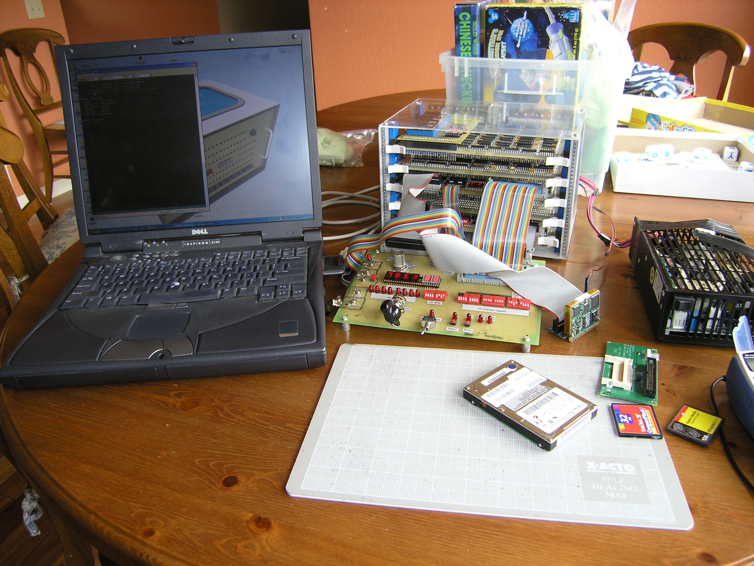
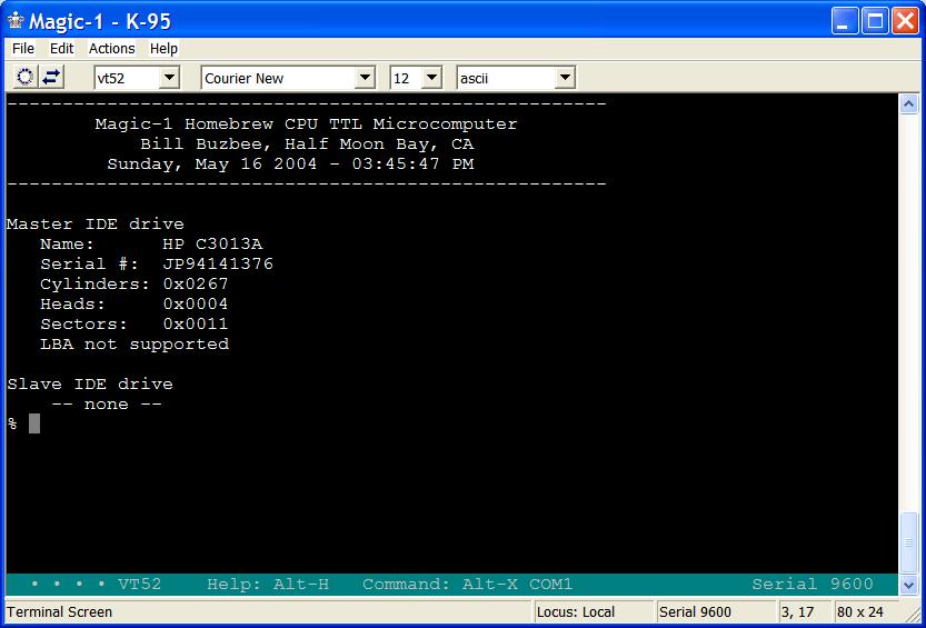
Note my new laptop desktop background: Alistair's M-1 ray-trace. Also, check out the tiny drive at the end of the IDE cable. It's an old 20 MB HP Kittyhawk microdrive. That thing was a bit of a sensation at the time it came out - the world's first 1.3" drive (in 1992) and is now used as a case study in business schools for how not to market breakthrough technology. Here's a window snapshot of the bios discovering the Kittyhawk:
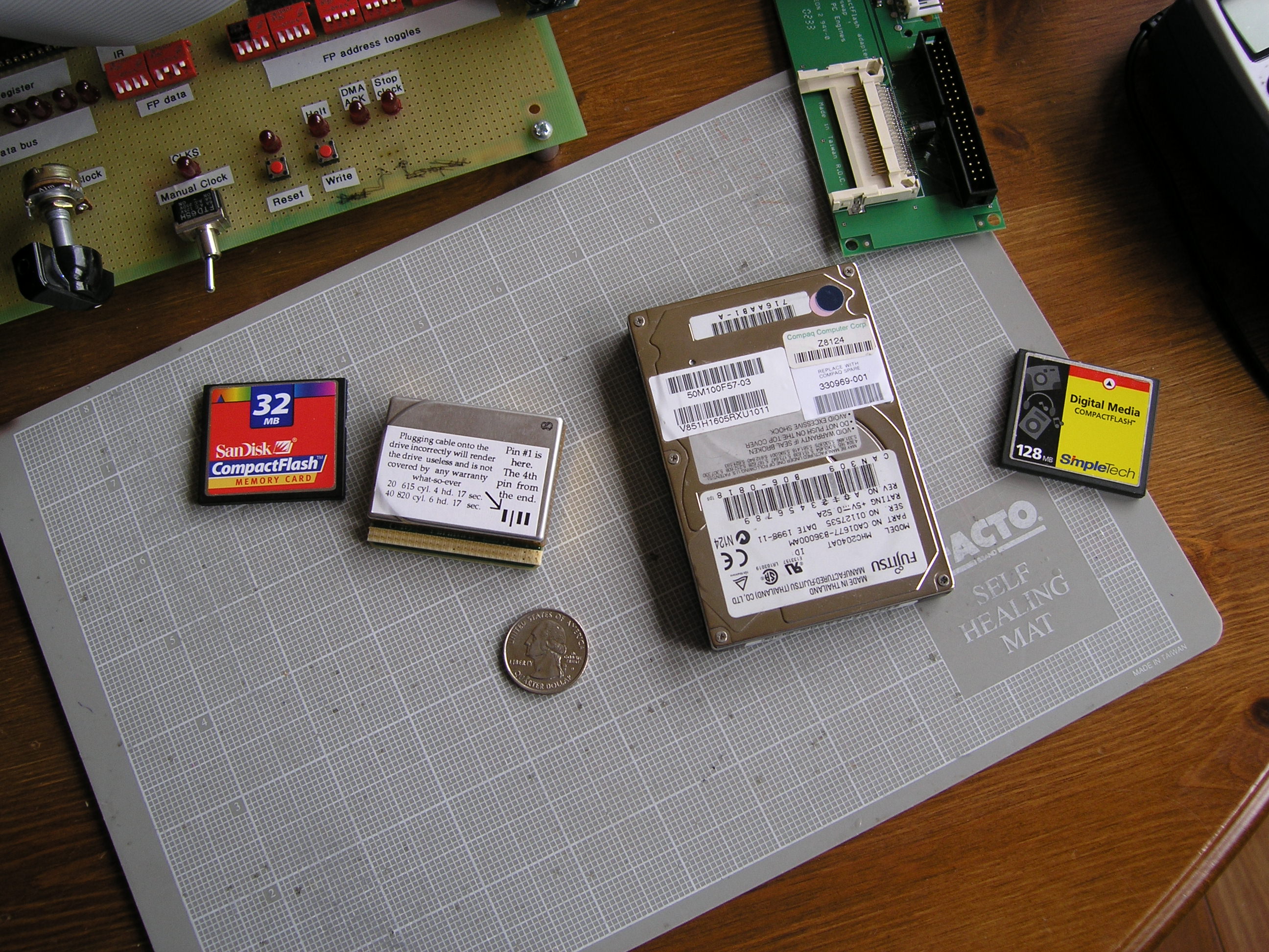
I also tried out some compact flash cards, and an old 4 GB drive from an old laptop of mine that died a few years ago. The Kittyhawk is in the middle, with a quarter for reference. My plan of the moment is to use the Kittyhawk as the primary drive, and then have a compact flash socket as the slave IDE device for backup purposes. The Kittyhawk is old enough not to support LBA addressing, so it will be a bit more difficult to use. However, I think the coolness factor makes it well worth the extra driver effort.
I still have a couple of things left to do on the hardware bringup front. There's still that UART wierdness where register outputs seem not to want to drive the bus high for more than a couple of seconds. In practice, this isn't a problem and my UARTs work just fine. However, it is odd and I want to make sure this isn't a symptom of a serious problem. Also, I still want to double-check my data bus behaviour. Once those things are done, I think I'll be ready to declare the hardware bring-up complete. I'll close out this web page and open up one for the continuing software bring-up. 5/13/2004Maia's costume is complete:
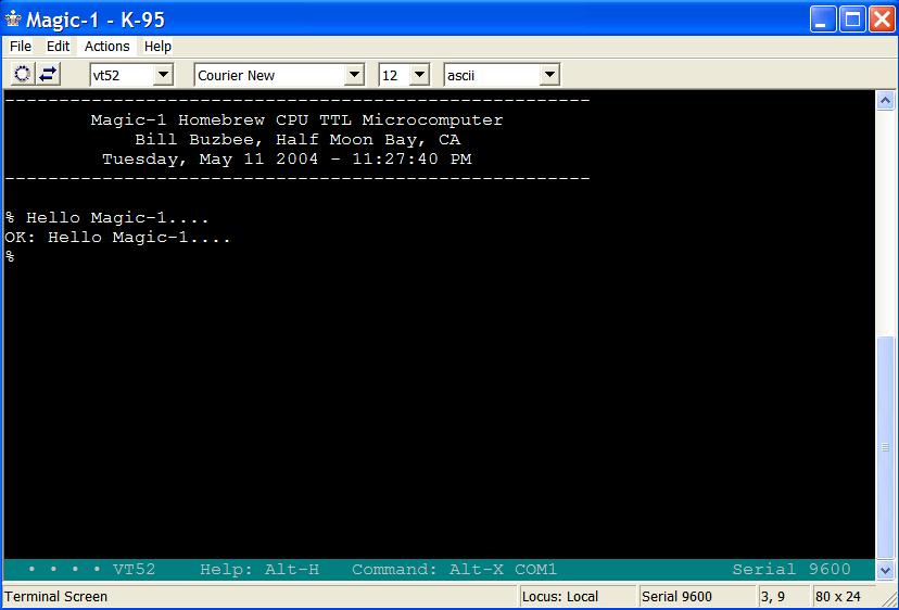
Now that's a far more impressive project than my silly computer stuff. Speaking of the silly stuff, I had just a few minutes to play yesterday so I tried out some IDE commands using a compact flash card as the drive. I got some behavior that clearly was wrong - the IDE RESET line was being activated every time I tried to read the IDE status register. A quick check of the wiring and code showed no apparent problems, so I tried swapping out the 8255 with another I had on hand. Oddly, that helped - the IDE RESET line behaved properly with the replacement part. I must have something something with my data bus wrong. The part I pulled was brand new; I really don't think it was faulty. One difference was that the one I pulled was a 82C55A-2, whereas the one that behaved more in line with my expectations was the non-CMOS version, a 8255A-2. Perhaps I've got a timing issue on the back (falling) edge of the system clock? Are new values getting put on the data bus just before _WR deasserts? The CMOS part should have latched in a LOW, but somehow got a HIGH instead. Will look into this in more detail this weekend. 5/11/2004Maia's costume is almost complete, so this coming weekend I should be able to resume hardware debugging. I have two primary items to explore. First, I want to verify that the shallow dip that showed up in the oscilloscope picture from 5/1/2004 is in fact an artifact of the data bus going from driven to floating. Counting the pulses, it seems to match what I remember the test microcode program - but not entirely. I would have expected two such dips. Can't be sure, though, as I no longer have that particular test microcode. Need to make sure I save everything. Anyway, I have a new set of test microcode written, and I should be able to confirm pretty quickly. The main thing I want to make sure of is that I don't have more than one device trying to drive the bus at a time. The second item is the strange behavior of the uarts. When I access the LSR (line status register) from the front panel, the two bits that tell you the transmitter is ready to send are both high (LSR==0x60) as they should be, but within a second or so they go low. If I deselect the chip and immediately reselect it, they come back high again. Both of my uarts behave identically here. One theory is that the uarts have some sort of timeout going on. Another theory is that I've got some flakey stuff going on and crap is getting clocked into the tranmitter. However, when I run programs, the uarts appear to be behaving just fine. I haven't been idle while the table is full of the 1950's pink poodle skirt. I've done quite a bit of work on the C compiler and assembler. I'm pretty pleased with how the C compiler (lcc) work has been going. I know I have quite a few problems to take care of for 32-bit integers and floating point data, but the 16-bit int and char support seems pretty solid. I can compile dhrystone now, but will need to do a lot of work on putting together libc and runtime support code. I also rewrote my beginning bios code in C. It's pretty much throw-away code, but I have routines to input and output characters and strings through the serial ports, send data to the post code display and - very cool - get and display the time and date from the real-time clock. The real-time clock seems to be working fine, though I am a little suspicious of my battery back-up circuit. The first 3-volt lithium battery I put in drained. That shouldn't happen for years. I'm hoping that the battery drain was a result on an accidental short of the pins on the wire-wrap side of the board. That would happen pretty easily if I put the board down on a conductive surface. Anyway, the current state of the bios is that it displays a hello message, the current time and date and then falls into a mode in which it inputs a line of text and then echos it back. Here's a screen snapshot:
After the debugging of the uart and data bus strangeness, I'm going to check out the IDE interface. I'm not going to do too much there, but if I remember correctly it should be a fairly simple matter to get a hard drive to transmit its identification info. I'll add bios code to look for a drive, and then display its info. I'm still looking around for an instrument case to put this thing in. The current plan (thanks for the suggestions Alistair) is bolt my card cage directly inside of a 6U instrument case. I found something close in a local surplus store, but it was a bit ragged. Will keep looking. Oh, also been thinking about Forth. I'll do a Forth for M-1 shortly, probably direct threaded. The main issue now is deciding on register assignment. My current thought is to use C as the instruction pointer, B as W and leave A as a scratch register. I'd use DP for the control stack and SP for the data stack. I have plenty of opcode space for some dedicated Forth instructions, but not a lot of microcode space - only 22 microinstruction slots. Should be enough for NEXT, DOCOLON and a couple of others. I'm a bit torn on what Forth to use. Andrew Holme sent me his Fig implementation, and I've also been looking at CamelForth - which is closer to modern standards. And, just to mix things up, I'm toying with the idea of redoing a Forth variant that I did long, long ago for my TRS-80. Is was based on (and basically copied out of) a Byte Magazine book: Threaded Interpretive Languages, by R.G. Loeliger. That book is what first got me excited about computer languages, interpreters and compilers long ago. 5/8/2004Lost the use of the kitchen table again. Monica finished the costume for Maia's kindergarten production, but accidentally ruined it with a too-hot iron - so she's having to do it all over again. So, I've been poking around with the tool chain. Back in the early 80's, Byte Magazine published a set of small CPU benchmarks. The benchmarks themselves are pretty worthless using today's standards, but I thought it would be fun to compare Magic-1 to some of the early 80's machines. It's not a fair comparison - I'm using vastly faster memory than was typically available then - but what the hell.... Anyway, the most famous of the Byte bencharks was the Sieve of Eratosthenes - a prime number generator. I found a copy and stripped out all of the timing, error-checking and target dependent code. Here's what's left: #define SIZE 8191 #define M (SIZE+1) #define N 10 #define TRUE 1 #define FALSE 0 int
main() {
int i,prime,count,k;
int iter;
static char flags[M]; for (iter=1; iter <= N; iter++) {
count = 0;
for (i=0; i <= SIZE; i++) {
flags[i] = TRUE;
}
for (i=0; i <= SIZE; i++) {
if (flags[i]) {
count++;
prime = i + i + 3;
// remove all multiples of prime
for (k=i+prime; k <= SIZE; k+=prime) {
flags[k] = FALSE;
}
}
}
}
//printf("Count: %d, 0x%x\n", count,count);
return(count);
}
I'm having main "return(count)" to ensure the result winds up in register A - my integer return register, and the benchmark is set up to do 10 iterations - each of which should find 1899 primes. Given that I already have a C compiler, I thought this would be easy - just compile and go. However, the exercise led me to find and fix several microcode bugs, two C compiler problems and do some enhancements to my hack assembler. However, it works now (at least in simulation - have to wait for kitchen table space to try it on real hardware). Following is the assembler listing, with embedded source code. I've highlighed the original C code in red. Note that loop code is embedded at the beginning and end of loops, so you'll see some duplication. Also, this is a one-pass assembler which generates the listing as it goes, so forward references show up as "----" in the code listing. You can find the final values in the fixup section, which is generated at the end when forward references are backpatched. Overall, the code quality isn't too bad considering that I haven't done much tuning and lcc really isn't an optimizing compiler. Until I get a linker up and running, I'm also having lcc inject some startup code, including a placeholder for the interrupt vector. Based on short runs on my simulator, I expect to complete 10 iterations in about 4.7 seconds on M-1 running at 3.68 MHz. Also, for this workload I'm averaging one M-1 instruction every 5 clocks. In real terms, that means I'll be running somewhere between .5 and .75 million instructions per second - though that metric has little to do with the [in]famous Vax MIPs rating. Eventually, I'll run dhrystone on this beast. Just for kicks, I tried compiling dhrystone, but failed about 90% through the main file. Another C compiler retargeting bug to track down. Anyway, here's sieve: : | ; Magic-1 assembly file, generated by lcc 4.2
: | _start:
0000 : 83 ---- | br over_ivec
0003 : ---- | defw unhandled_exception ; Interrupt vector 1
0005 : ---- | defw unhandled_exception ; Interrupt vector 2
0007 : ---- | defw unhandled_exception ; Interrupt vector 3
0009 : ---- | defw unhandled_exception ; Interrupt vector 4
000b : ---- | defw unhandled_exception ; Interrupt vector 5
000d : ---- | defw unhandled_exception ; Interrupt vector 6
000f : ---- | defw unhandled_exception ; Interrupt vector 7
0011 : ---- | defw unhandled_exception ; Interrupt vector 8
0013 : ---- | defw unhandled_exception ; Interrupt vector 9
0015 : ---- | defw unhandled_exception ; Interrupt vector a
0017 : ---- | defw unhandled_exception ; Interrupt vector b
0019 : ---- | defw unhandled_exception ; Interrupt vector c
001b : ---- | defw unhandled_exception ; Interrupt vector d
001d : ---- | defw unhandled_exception ; Interrupt vector e
001f : ---- | defw unhandled_exception ; Interrupt vector f
: | unhandled_exception:
0021 : 00 | halt
: | over_ivec:
0022 : 7c 8000 | ld.16 a,0x8000
0025 : cb | copy sp,a
0026 : 7c 4000 | ld.16 a,0x4000
0029 : b6 | copy dp,a
002a : 80 ---- | call _main
002d : 00 | halt
: | bss
: | L2:
: | defs 8192
: | global _main
: | cseg
: | _main:
002e : e5 f4 | enter 12
: | ;main() {
: | ; for (iter=1; iter <= N; iter++) {
0030 : 7a 01 | ld.16 a,1
0032 : d9 04 | st.16 -10+14(sp),a
: | L3:
: | ; count = 0;
0034 : 7a 00 | ld.16 a,0
0036 : d9 06 | st.16 -8+14(sp),a
: | ; for (i=0; i <= SIZE; i++) {
0038 : 7a 00 | ld.16 a,0
003a : d9 0a | st.16 -4+14(sp),a
: | L7:
: | ; flags[i] = TRUE;
003c : 81 0a | ld.16 a,-4+14(sp)
003e : 74 002e | lea b,L2(dp)
0041 : 3f | add.16 a,b
0042 : 79 01 | ld.8 b,1
0044 : d6 00 | st.8 0(a),b
: | ; }
: | L8:
: | ; for (i=0; i <= SIZE; i++) {
0046 : 81 0a | ld.16 a,-4+14(sp)
0048 : 3d 01 | add.16 a,1
004a : d9 0a | st.16 -4+14(sp),a
004c : 81 0a | ld.16 a,-4+14(sp)
004e : bc 1fff ea | cmpb.le.16 a,8191,L7
: | ; for (i=0; i <= SIZE; i++) {
0052 : 7a 00 | ld.16 a,0
0054 : d9 0a | st.16 -4+14(sp),a
: | L11:
: | ; if (flags[i]) {
0056 : 81 0a | ld.16 a,-4+14(sp)
0058 : 74 002e | lea b,L2(dp)
005b : 3f | add.16 a,b
005c : 12 00 | ld.8 a,0(a)
005e : 95 -- | cmpb.eq.8 a,0,L15
: | ; count++;
0060 : 81 06 | ld.16 a,-8+14(sp)
0062 : 3d 01 | add.16 a,1
0064 : d9 06 | st.16 -8+14(sp),a
: | ; prime = i + i + 3;
0066 : 81 0a | ld.16 a,-4+14(sp)
0068 : d9 02 | st.16 -12+14(sp),a
006a : 85 02 | ld.16 b,-12+14(sp)
006c : 3f | add.16 a,b
006d : 3d 03 | add.16 a,3
006f : d9 08 | st.16 -6+14(sp),a
: | ; for (k=i+prime; k <= SIZE; k+=prime) {
0071 : 81 0a | ld.16 a,-4+14(sp)
0073 : 39 08 | add.16 a,-6+14(sp)
0075 : d9 0c | st.16 -2+14(sp),a
0077 : 83 ---- | br L20
: | L17:
: | ; flags[k] = FALSE;
007a : 81 0c | ld.16 a,-2+14(sp)
007c : 74 002e | lea b,L2(dp)
007f : 3f | add.16 a,b
0080 : 79 00 | ld.8 b,0
0082 : d6 00 | st.8 0(a),b
: | ; }
: | L18:
: | ; for (k=i+prime; k <= SIZE; k+=prime) {
0084 : 81 0c | ld.16 a,-2+14(sp)
0086 : 39 08 | add.16 a,-6+14(sp)
0088 : d9 0c | st.16 -2+14(sp),a
: | L20:
008a : 81 0c | ld.16 a,-2+14(sp)
008c : bc 1fff ea | cmpb.le.16 a,8191,L17
: | ; }
: | L15:
: | ; }
: | L12:
: | ; for (i=0; i <= SIZE; i++) {
0090 : 81 0a | ld.16 a,-4+14(sp)
0092 : 3d 01 | add.16 a,1
0094 : d9 0a | st.16 -4+14(sp),a
0096 : 81 0a | ld.16 a,-4+14(sp)
0098 : bc 1fff ba | cmpb.le.16 a,8191,L11
: | ; }
: | L4:
: | ; for (iter=1; iter <= N; iter++) {
009c : 81 04 | ld.16 a,-10+14(sp)
009e : 3d 01 | add.16 a,1
00a0 : d9 04 | st.16 -10+14(sp),a
00a2 : 81 04 | ld.16 a,-10+14(sp)
00a4 : bd 0a 8d | cmpb.le.16 a,10,L3
: | ; return(count);
00a7 : 81 06 | ld.16 a,-8+14(sp)
: | L1:
00a9 : 0d | pop sp
00aa : 0b | pop pc
: | end
=========================== Fixups =================================
Fixup applied, 2-byte store of 0x0010 to 0x0078
Fixup applied, 1-byte store of 0x0030 to 0x005f
Fixup applied, 2-byte store of 0x0001 to 0x002b
Fixup applied, 2-byte store of 0x0021 to 0x001f
Fixup applied, 2-byte store of 0x0021 to 0x001d
Fixup applied, 2-byte store of 0x0021 to 0x001b
Fixup applied, 2-byte store of 0x0021 to 0x0019
Fixup applied, 2-byte store of 0x0021 to 0x0017
Fixup applied, 2-byte store of 0x0021 to 0x0015
Fixup applied, 2-byte store of 0x0021 to 0x0013
Fixup applied, 2-byte store of 0x0021 to 0x0011
Fixup applied, 2-byte store of 0x0021 to 0x000f
Fixup applied, 2-byte store of 0x0021 to 0x000d
Fixup applied, 2-byte store of 0x0021 to 0x000b
Fixup applied, 2-byte store of 0x0021 to 0x0009
Fixup applied, 2-byte store of 0x0021 to 0x0007
Fixup applied, 2-byte store of 0x0021 to 0x0005
Fixup applied, 2-byte store of 0x0021 to 0x0003
Fixup applied, 2-byte store of 0x001f to 0x0001
=========================== Symbols =================================
L1 -> 0x00a9
L4 -> 0x009c
L12 -> 0x0090
L18 -> 0x0084
L17 -> 0x007a
L20 -> 0x008a
L15 -> 0x0090
L11 -> 0x0056
L8 -> 0x0046
L7 -> 0x003c
L3 -> 0x0034
L2 -> 0x002e
_main -> 0x002e
unhandled_exception -> 0x0021
over_ivec -> 0x0022
_start -> 0x0000
5/3/2004M-1's serial ports are working. From time to time I've casually tried to set and examine the 16550 uart control registers through the front panel, but what I read never seemed to make any sense. This evening I went into serious debugging. I used the logic probe to test every pin, I double-checked the datasheet (for about the 20th time), I found similar schematics - and everything looked like it ought to work. However, whenever I tried reading the line control register via my front panel switches, I got what seemed to be nonsense. I would get a few LEDs lit, but after two or three seconds they would just go out. I assumed that meant for some reason the UART wasn't driving the bus when it should be - leading me to do lots of probing around device select. Once, however, when switching between my two uarts, I realised that the brief LED pattern started off at what I would expect (0x60 for the LCR). It occurred to me that perhaps the uart is not designed to hold continous data reads, and was shutting off it's data output after a few seconds. So, I went ahead and wrote a small program to output a "Hello World!" and "Hi Mom!" strings from each of my two serial ports. Burned the ROM, hooked up my laptop and turned it loose. Damn thing was working all along:
Picture is a bit blurry, and it seems the C compiler (lcc) I retargeted for Magic-1 is using Unix line end conventions, but it works! Next up is to test input - I'll probably just do an echo program. One thing I will need to address soon, though, is a slower clock speed for dealing with devices (the datasheet says the real-time clock can require up to 1ms after select). I originally planned to have a "wait state" bit in the page table, and arrange that any access on a page marked with that bit would get a stretched out one or more clock cycles to allow extra time for accessing slower devices. At the time I designed the clock circuitry, though, I has having enough trouble just getting the simple circuit right so I decided to put off wait state generation until later. Well, now it's later. I'm having second thoughts about doing this as a page attribute, though. In many ways it is more elegent, and I even have a couple of page table bits free so I could cause 0..3 wait states to be inserted. A likely simpler appoach, though, would be to add a bit of memory (flip-flop) in device space. If I stored a 1 to this flip-flop, the system clock would be divided by 4 (or 8 or something) to send the machine into slow mode. When writing a zero, it would speed up again (or actually, do that reverse - 0 is slow, and the FF is cleared on _RESET - that way the machine starts off slow, which could be useful if I were using slow boot EPROM). It would be the responsibility of the device drivers to explicitly slow down the clock before access, and then speed it back up again. Anyway, I haven't figured out the circuit changes needed for that solution either. I'm open to suggestions. 5/3/2004 [morning]Spent just a few minutes with the project yesterday. I had neither time nor kithen table space to get out the oscilloscope and check out address generation and setup, but I did cobble together a new memory stress test. The test program was pretty simple - just filled and loaded a pattern of 0x00, 0xff, 0x55 and 0xaa in a loop. I tried it out at 3, 3.15, 3.5, 3.67 and 3.75 MHz. Somewhat interesting results:
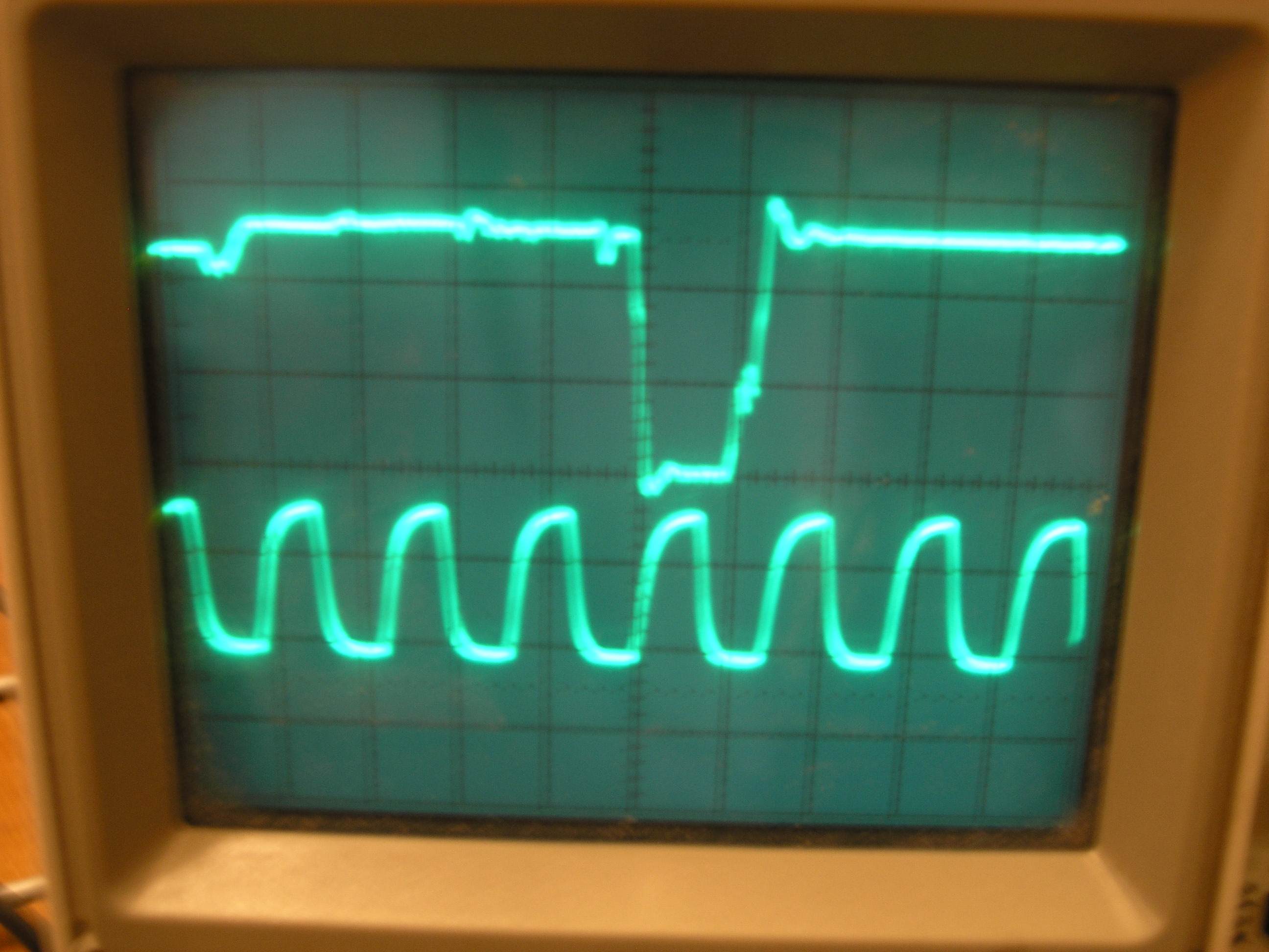
Most all of these results seem entirely consistent with my belief that my speed ceiling is due to memory load critical path: slowing down by 30ns with the slower memory caused failures, and the device SRAM decode path is 3 or 4 logic gates longer than the memory card SRAM decode path so I'd expect failures to show up there first. The real oddity is that I had failures at 3.5 MHz, but passed consistently at the faster 3.67, and then failed at 3.75. I suppose a theory here could be that 3.67 just happens to be in the trough of signal ringing, whereas 3.5 is at the peak. I'll understand a little better when I examine and measure address setup time and use a variable clock to dial in more precisely. One other thing I want to investigate further is the dip that shows up in the second of the 5/1/2004 oscilloscope trace pictures. Régis emails that it suggests two devices in conflict - one trying to push the line high and the other pull it low. I'll do a review of the schematics to see how this might be happening, and I can use the logic analyzer to test. I'm just about done with speed analysis. My goal here is to make sure I'm not leaving performance on the table because of a silly mistake and that I'm not suffering from signal integrity problems bad enough to cause flakiness at lower speeds. It looks like things are working just fine - the performance I'm getting is right in line with what I should expect from memory path length, and the signals I've seen so far look good enough. I expect my next experiments here to be the last ones, and I'm not planning on doing any re-work to try to speed up the memory path. Next up will get getting the serial ports functioning. I did a quick test of these a few days ago, and they aren't behaving as I expected. It's probably just pilot error. My early test stuck in a busy-wait loop on a load of the uart's line status register looking for the bit which says the UART is ready for the next byte to transmit. The bit never showed up. I'll probably start by searching for someone else's schematic which uses a 16550 uart to see if I hooked up all of the select and enable lines correctly. 5/1/2004Lucky for me, Monica had trouble with her sewing machine and packed up Maia's dress to finish over at her folks' house. So, I got to take control of the kitchen table and spend a couple of hours with M-1 and my oscilloscope. I'm not confident that I interpreted what I saw correctly, but it does now appear to me that my speed ceiling of somewhere between 3.0 and 3.5 MHz is a result of the critical path length of a memory load. In reviewing the schematics, this seems to make sense. When I computed my first critical path, MDR to L to ALU to Z bit, I added up the worst case times in the datasheet. In practice, the parts seemed to run a lot faster than worst case, and when I swapped out a few of them for fast 74F parts, I was able to push my speed up substantially. Overall, I was able to dramatically compress that path from the original worst-case 366ns calculation. The memory load path, though, appears to be a lot less compressable. I think when they say 70ns for memory access, they mean 70ns. At 4 MHz, I would need to get a stable address, select the proper device and read it all within 120 ns or so. Together, my SRAM and page table memory are rated for 85 ns, leaving me only 35ns for everything else. I'm not going to hit 4 MHz. Here's a picture to illustrate. The top trace is a data bus line taken where it is being consumed on the furtherst device. The picture is blurry, but care was taken to get the top trace - I took Dave Conroy's advice and solder-tacked down a bare wire on the groung pin of the probed device. I wrapped that wire around the barrel of the probe to give myself a really good ground - and got a nice crisp trace. The bottom trace is my main clock, ClK_S, running at 4 MHz. I just pulled this off of the backplane, and had a pretty long ground line so it looks a lot worse here than it really is. When carefully probed, it is nice and square. Anyway, the interesting part of the picture is the falling edge of the top trace. This represents the data line going 0 just before it's value is clocked into the device by a signal that shows up 10 or 20 ns after the rising edge of CLK_S just below it. Note how close those two edges are - not enough time, I think.
Now, also in looking at the data line signal, it appears to me that although you can see ringing, I don't think it's that bad. There was something else on the data bus line trace that I didn't understand. It was a regular dip in the voltage that showed up before the zero bit dip. Here's a picture:
This particular test did a lot of transitions between 0, 1 and a load where nothing was driving the bus. It's a little hard for me to correlate the osciloscope pictures with my test program, but I think that dip would be consistent with the data bus floating. Not sure, though. My next step is to either borrow a function generator, or cobble together a variable clock that runs between 2 and 4 MHz. I'd like to try diailing up the speed until a get a failure, and then see if that failure is consistent with a failed read. That will also give me the values to put into my clock dial. I'll put the fastest somewhat-reliable speed in the "fast" setting, and then back off 20 or 30% for the "normal" clock setting. 4/30/2004Monica is making a 50's-style dress for Maia (my 6-year-old) for next week's kindergarten production, so I've lost the use of the kitchen table. My next debugging session will have to wait. I have decided on a test plan, though. The experiment will try to answer two questions: how long does it take for my data and address busses to stop ringing - and are my failures due to a new speed path being violated. When I first looked for critical paths, the MDR to L to ALU to Z bit to MSW was the clear winner. Now, though, I think I may have a speed issue on the loading of a byte of memory into the instruction register. The parts should be fast enough (barely), but if it takes a substantial amount of time for ringing to subside on either or both of the address and data busses, I could be in trouble. My last session used special microcode to really focus on the topic in question and went well enough that I decided to do it again. What I've got is a tight microcode loop which does some register-only initialization, then a series of 7 byte loads one after another, followed by a loop back to start over. The load sequence goes through all interesting transitions between load a data value of 0, 1 and floating. By making this test microcode-only, I also have the ability to run it on my device rom and sram (by switching the front panel rom/sram switch). The data values loaded will be in addresses 0 and 1, and I can play with those. Because I'll be using the oscilloscope for this, I also have the microcode generate a special signal (INIT_INST) just before the loads start. That will serve as the trigger. Here's the interesting part of the test microcode:
0x100, 0x101 and 0x102 do initialization - register A gets 0x8001 (an address in device space that maps to nothing), MDR is reset to 0 . MAR starts off as 0 (cleared at _RESET), and this test program should make sure it is zero again when we loop back. Starting at 0x103, we do a series of loads, as follows:
This sequence should cover all of the interesting combinations. 4/29/2004Interesting debugging session tonight. My goal was to identify whether what I believe is the critical path is the cause of my failures above 3.something MHz. To do this, I used my logic analyzer in timing mode. By looking at the schematics, I believe my longest path is the one that generates the Z bit following an arithmetic operation that takes the MDR as the left operand. What I wanted to see is how long after the Z bit is generated does a latch signal arrives which consumes it. This also suggested a 2nd experiment: latch signal window size. I'm probably not using common terminology, but I divide my control signals into two groups: enable signals and latch signals. The enable signals are what determine which registers contents are sent to the ALU, which ALU operation, etc. These signals are unclocked, and are expected to bounce around a bit before settling down. The only restriction is that they settle down and their actions take effect before a latch signal arrives. In my terminology, a latch signal is the clocked signal which causes an edge sensitive device (such as the flip-flops I use to build registers) to take a new value. These signals cannot bounce around, and are in some way combined with CLK_S - the system clock. Anyway, in an ideal world, all of my latch signals would arrive at the same time. In practice, they don't. Some are generated by AND'ng directly against CLK_S, others go through one or two demuxes which use CLK_S as an enable. So, my second experiment is to determine the length of time between the fastest latch signal and the slowest. This window is important because it is conceivable that a device which clocks in a new value on an early latch signal might release its contents into the system in such a way that state is disturbed before a slower latch signal arrives. Also, when looking at critical path timing, I want to make sure that my critical path generates its results in time for the earliest possible latch signal to consume it. Now, to make this a tight experiment, I wanted to eliminate as much other stuff as possible. In particular, I wanted to avoid considering any memory issues. So, I created a special set of microcode which generated the signals for my critical pach and does little else. No memory accesses are made at all - just a tight microcode loop. I am able to do meaningful arithmetic operations using this technique because my microcode instructions are capable of delivering immediate values 1, 0, -1 and -2. Here's the microcode:
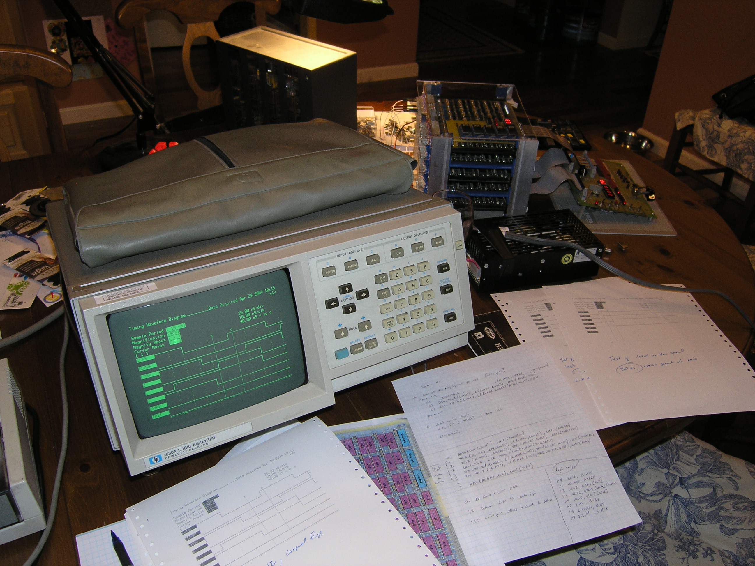
Instruction 0x100 clears MDR to set things up. 0x101 and 0x102 are two variants that will show the elapsed time between the fastest latch signal (L_PAGING) and the slowest (L_MSW). There are two variants because L_MSW can be generated in two ways. Instructions 0x103, 0x104 and 0x105 perform simple arithmetic operations, generate flags, and eventually return MDR to 0x0000 before branching back to start. The idea would be to run this microcode and then measure the time between interesting events. Here's what the kitchen table looked like after setting things up:
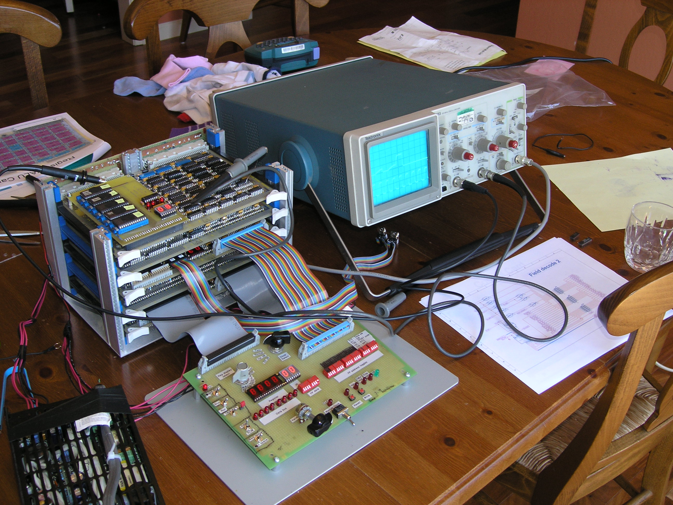
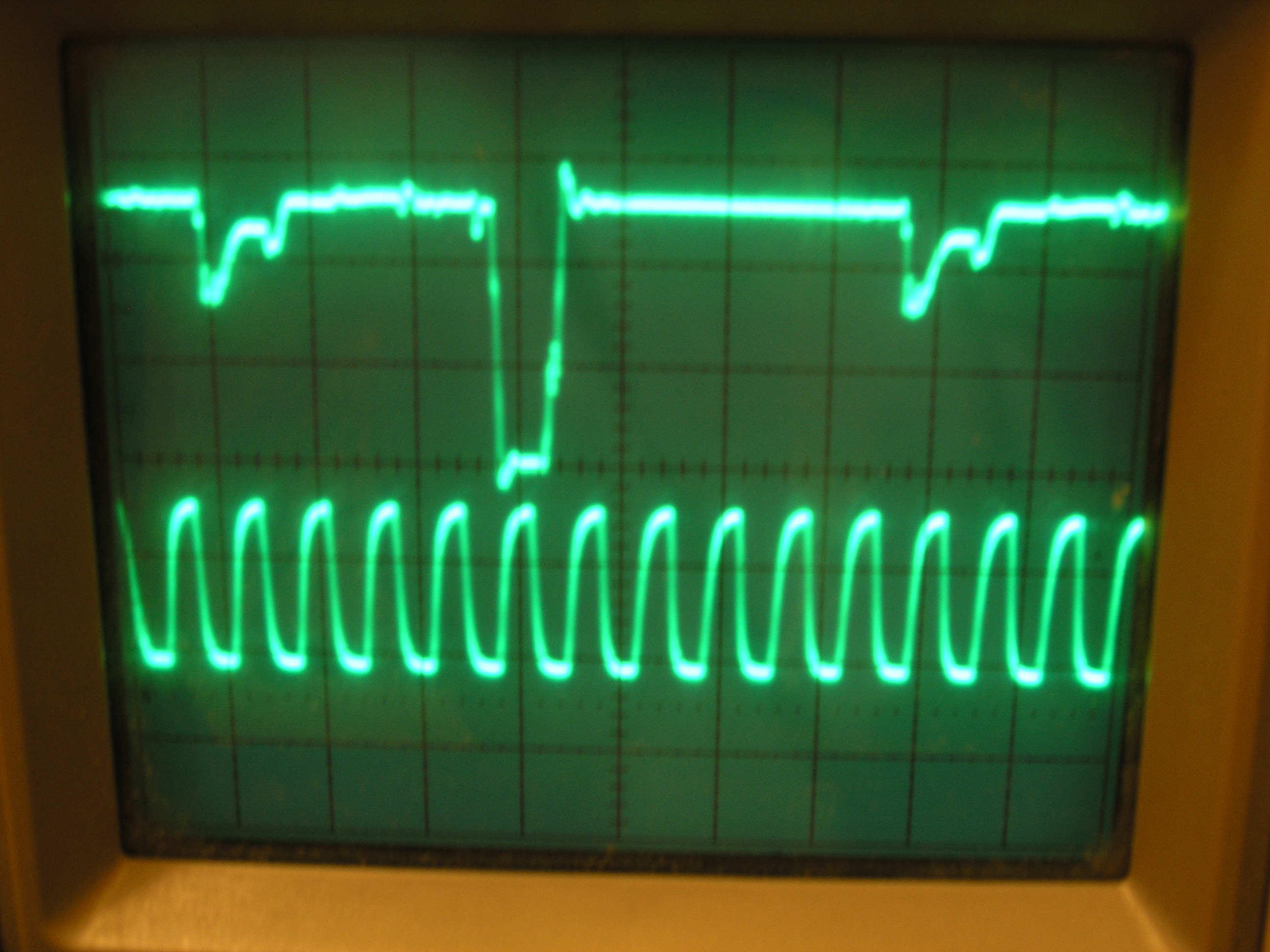
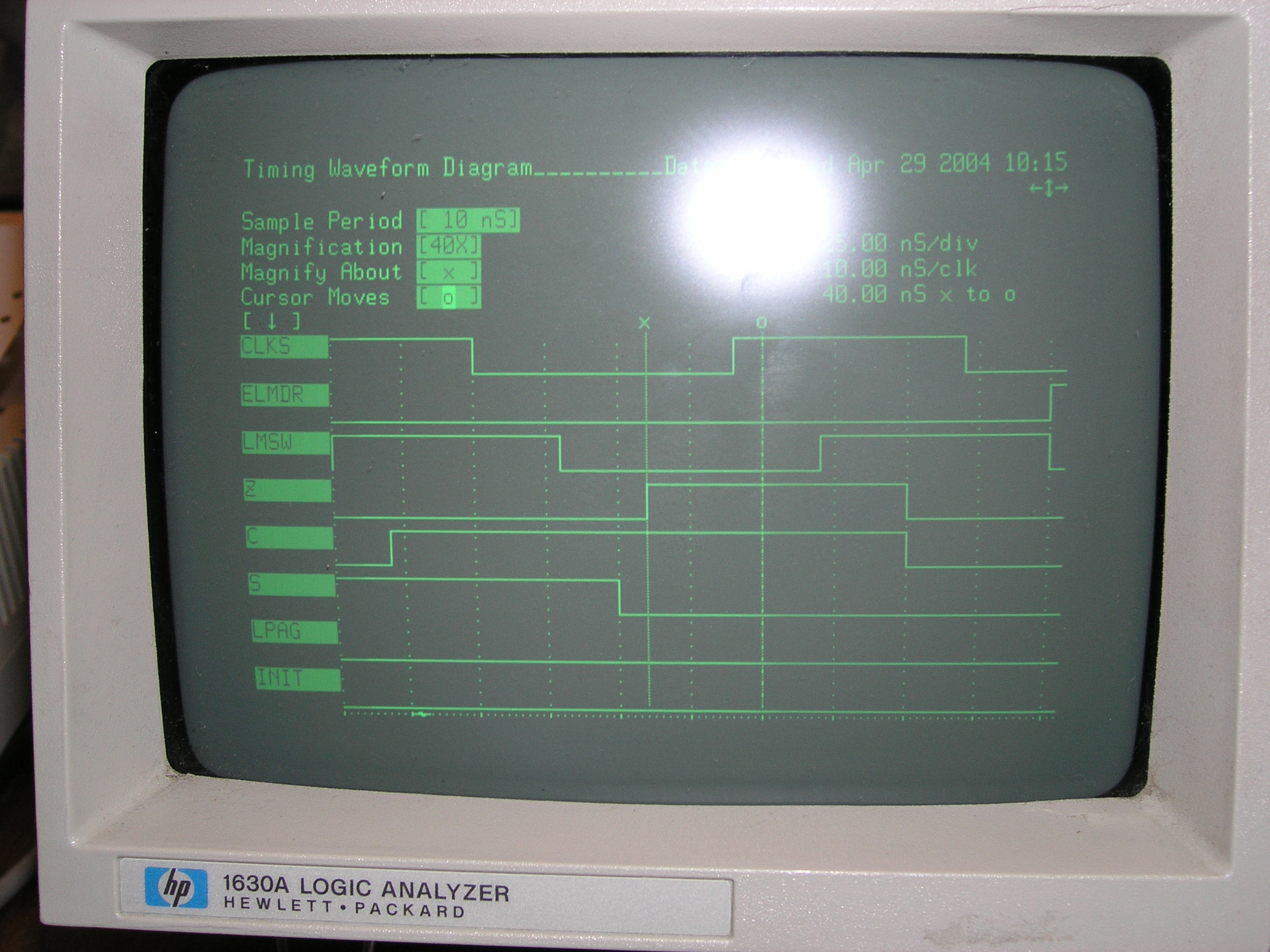
And now, the results: I don't believe I have a critical path problem for MDR->ALU->Z flag. Although my logic analyzer has only 10ns resolution, it appears that the Z bit was being generated with plenty of time to spare. Even at 6 MHz, the Z bit was ready 60ns before the L_MSW rising edge arrived. At 4 MHz, it looked like we had about 90 ns. For an LS part, we only need 5ns or so setup time. For the other experiment, it appears I have about a 20 nanosecond window between the first and last of the latch signals. So, if we subtract that 20 ns to account for the fastest latch signal, and 5ns for setup time - that still leaves 65ns at 4 MHz. Here's a lousy picture of the 6 MHz run (still trying to figure out how to take good pictures with the digital camera).
The "x" vertical bar is positioned where the Z bit materializes, and the "o" bar is positioned where the first of the latch signals could arrive. This was the 6 MHz run. So, based on this I think I can eliminate a missed critical path in this part of the clock cycle. The next experiment should probably be something to either finger or eliminate decoupling problems or data/address bus termination issues. Not sure yet how to proceed there.
4/29/2004 [morning]Mea culpa. Compared with hardware engineers, software developers have a reputation of being pretty undisciplined. Looking at the way I've been probing the speed possibilities of M-1 over the last few days, I have to admit I'm living up (..or down) to the image of a software hack. Things started off pretty well - I had a good baseline with 74LS parts. My clocks looked great on the oscilloscope, and M-1's performance looked pretty good. I had calculated a worst-case speed path of 366 ns, and in practice was consistently passing the looping validation suite at 2 MHz (which would allow for a 250 ns critical path. That seemed reasonable to me, given the conservative nature of the worst-case calculations. My next step was fine - I replaced a half-dozen or so LS parts on what I believed was the critical path with F versions, and was able to push to 2.5 MHz. However, when I added a few more F parts, the machine stopped working altogether. This is where the software guy in me took over. Instead of stopping and determining why the machine stopped working, I just pulled those new F parts, and replaced a different set of chips. Things went back to working for a while, and then I had another instance of a chip replacement causing failure. Did I stop and figure out why? No - decided to just replace everything with F, fire it up and see what happens. This is typical in the software world. Something odd? Just yank it out, add different code, fire it up and see what happens. Given the rapid cycle time of edit/compile/debug, it's easy to see how this behavior developed. However, it's not a good thing. Too many problems get passed over. With the speed exercise for M-1, I have to remember that my goal is not to push the machine to a top speed, but rather to characterize it. I want to know how fast it will go, and why it will only go that fast. Is it critical path length, or perhaps noise on my unterminated address and data busses? I'm not going to know if I just randomly swap parts. Anyway, I've backed out my "all-F" plan, and now have just F parts in the places I believe affect the speed path. My next task will be to write some test programs that exercise what I think that speed path is, and take a look at the signals using the timing mode of my logic analyzer. That should tell me if I know what my true critical path is, and if it's the reason for my speed ceiling. 4/28/2004Continued with the experiment of using mostly all 74F series parts to bump up the speed. Several folks have emailed me to suggest that I'm probably heading for trouble with power, decoupling and termination near 4 MHz with all F parts (thanks Ben & Mark). They may be right. This morning, I tried 3.75 MHz and it seemed quite solid. I let my validation suite loop for a good hour and it passed nicely. This evening, I completed the updating of most all parts to 74F series. I pass one-shot runs of my validation suite at 3.75 MHz, but I don't live for long in the looping version. I've backed the clock down to 3 MHz, and it seems very happy. I'll address the decoupling issue first. I have a bag of .01 uF caps that I'll solder down this weekend. We'll see if that helps. If not (and perhaps even if so), I'll also break out the logic analyzer again and try out it's timing capabilities. 4/27/2004 (morning)Discovering that fiddling with speed paths is tricky. I started swapping in "F" parts along my critical path, but ran into timing problems. I tightened up my critical path (L bus enable though ALU through condition code setup) so much that my L bus enable signals got in front of my latch signals, causing failure. So, I then had to tighten up my latch signals, which got something else out of whack. In the end I decided to see what would happen if I swapped out just about everything and made the machine largely F parts. At the moment, I'm about 80% F (the rest LS). Today I'll pick up a few more F parts to make the machine consistently 74F series and then see if that will get me to 4 MHz. I'll decide later whether I want to stick with my original plan to make Magic-1 largely vanilla 74xx series. It was a nice thought, but I think I like the idea of a faster machine better. We'll see. Besides just using faster parts, I have identified a couple of areas in which I could shave some time by circuit cleanup. I'm not inclined to do that now, but if I'm right on the edge of hitting 4 MHz, I might. I can consistently pass my fibonacci test at 4 MHz, but fail the validation suite. I seem to consistently fail at the same point, which is good. I haven't looked in detail at the faling point, but when I get a chance that should make it clear where my new speed path is (and I suspect it's still the condition code path). In any event, the machine is doing very well. I ran it all night running the validation suite in a endless loop at 3.67 MHz. After putting in the last of the F parts, I'm going to add some additional decoupling capacitors. Right now I've got 0.1 uF ones on every other position on the boards. My understanding is that 0.01 uF is best for F series parts, so I'll add a bunch of those in the unused position. Also, it's time to start testing out the serial ports. I'd like to start talking with this machine. 4/25/2004Took a few days off of the project to attend to the rest of my life, but resumed with a marathon debugging session Saturday afternoon through Sunday morning. The speed problem is solved. It turns out that the SRAM on the device card wasn't grounded. Amazingly, it still functioned at low speed - presumably via current flowing through signal pins. Once that ground wire went in, the machine immediately started running at 1 MHZ. With some more fiddling, it's now running at 3 MHZ. By replacing some of the slower devices on the speed path (register->L bus->ALU->flags->mux->flag register), I'm confident we can hit my original target of 4 MHZ. Don't think we'll get much faster than that, but in truth I would have been happy at anything over a megahertz. As with the rest of this project, I had big assistance in the latest push. Special thanks to Mark Atherton, Dave Conroy and Al Kossow. Mark's advice saved me from redoing the backplane and helped yeild clean signals. Dave came over and sat down with me at the kitchen table in front of an oscilloscope and logic analyzer for a 4+ hour intense debugging session that got us to within inches of the eventual problem. And Al, a full week ago, correctly diagnosed the problem after hearing me describe the symptoms. Unfortunately, when he said "did you double-check to make sure everything is grounded?", I answered yes. In fact, I had - but I beeped out the connections on the wire-wrap side of the board. I expect that my probe brushed past the adjacent groung pin giving me the beep I was looking for. My digital camera is still a bit flakey, but I was able to coax it into a few pictures. Here's what my wife has to put up with, the aftermath of the debugging session with Dave Conroy:
I picked up the logic analyzer on eBay a year or so ago for about $100. Well worth it. Besides being a really cool geek toy, it was phenomonally useful. Here's the set-up that delivered the smoking gun report that pointed to a problem with the SRAM chip:
Finally, here's a picture of the reworked backplane, after tacking down the ground and power lines as Mark Atherton suggested. After doing this, my signals looked a lot cleaner.
4/18/2004The new digital camera appears to have lost its mind - so no pictures today. I did a bit of soldering today, tacking down a wire from each ground pin on the back plane to the backplane copper ground sheet. I hope that will improve my ground distribution, but there was no apparent improvement in the machine's ability to run at 1 Mhz. I also ran a dedicated power cable out to the temporary front panel. Previously it had been getting power through the ribbon cable. My plan for the real front panel assembly was always to have a dedicated power input, but I got lazy for the temporary one. It still runs a bit lower voltage than the rest of the machine (4.92 vs 4.98) because I did some poor daisy-chain wiring on the HP hex displays (which really suck power). I reworked the resister/capacitor combo on the 555 timer that generates my variable clock. Instead of a top speed of 410 Hertz, it now goes up to 4.7 kilohertz. I also added a 74LS74 flip-flop to give me divide-by-2 and divide-by-4 capabilites for one of the oscillators. With this, I was able to determine that M-1 runs pretty reliably at 490 kilohertz. Still a factor of 10 off of where I'd like to be. I want to finish up some scheme to increase the number of power feeds into the backplane, and after that will begin addressing signal integrity. 490 kilohertz isn't bad for a hobbiest homebrew, but I think this machine should be able to run a lot faster. Also, hope to be able to spend some cycles making progress on the front panel and enclosure. 4/16/2004Just spent a few minutes with the project tonight. First, good news - I added four more tests to the validation test EPROM and they all passed. Those tests covered basic operation of the paging and hardware address translation mechanism. I'm quite happy that worked - it means I am successfully reading and writing the special page table memory. I also burned a copy of the tests that just loops forever. I'll let that run overnight to see how stable things are. I dug out my old HP nixie-tube frequency counter and hooked it up to measure the slow variable clock. At full speed with the slow clock, Magic-1 is humming along at 410 Hertz (not Khz, Mhz or Ghz - just Hz). Given my recollection of the typical number of clocks needed for an instrucdtion, that would put M-1 at about 80 instructions a second. Woo - speed burner! Tommorrow I'll try to finish off the cleanup of the power and ground distribution, and after that I'll adress the clocks. I looked at my 1 and 4 Mhz clocks tonight with an oscilloscope, and they don't look very good. The 1 Mhz clock has pronounced squiggles on the corners, and a subtle squiggle midway through the flat part. The crest of the falling-edge squiggle bounce appears to be about .3 to .4 volts high. The 4 mhz clock is just a mess of squiggles - they just don't get a chance to settle. I have a termination scheme in place - I'm running those signals through a resistor before they go out onto the bus. It's 68 ohms now, and I'll play with that value to see if I can de-squiggle things. I'm having trouble with my digital camera, but hope to post pictures of the clocks as they appear on the scope soon. Ben Franchuk also pointed out that I am not terminating my memory bus, and passed along a really interesting web reference to termination problems and solutions: http://pluto.njcc.com/~hjohnson/s_term.html. I guess I may have a lot of termination issues to work through (at least assuming I want the machine to run faster than 80 instructions per second :-). 4/15/2004Have begun addressing the power supply and distribution issues. First off, I built a heftier wiring harness and got out the $2 surplus power supply I picked up for M1 a year or two ago. I may end up not using it - it's single supply (5V @25A - way more current than I need). The issue is that I'm probably going to need a fan in the box, and I think most of those run at 12 or 24 volts. For now, though it works quite well. The wiring harness took care of the bulk of my voltage problems. Previously I was getting somewhere between 4.7 and 4.8 volts on the cards (and down to 4.6 on the temporary front panel). Now, I get 4.96 volts on the cards. I think that's good enough for now. I still have to run mostly using the slow variable speed clock. For the fibonacci test program, I can pretty consistently pass when using the 1MHZ clock, but never with the 4MHZ one. For the big validation test, though, I've never yet succeeded at either 1 or 4 MHZ, but it consistently passes using the slow clock. Before I dig into this, I want the address the rest of the power distrubtion issues (though just for jollies, I will probably dig out the oscilloscope and take a look at the clock). The next, and probably bigger issue, is the lack of distributed ground lines. I have plenty of lines allocated in the backplane, but only one from each card is actually connected to either power or ground (via a 22awg wire). I knew this was a problem earlier, and had pretty much convinced myself I needed to do some custom PCBs to sandwitch over the existing wire-wrapped backplane to supply power and ground to all of the appropriate pins. However, Mark Atherton suggested that I use the PCB approach as a last resort, and try running wire-wrap wire from each of the appropriate backplane pins to the ground & power planes on the backplane. I'd wrap the pin end of the wire, and solder down the other end. I thing I'll try this. It will be a bit tricky - there isn't a lot of room left on the backplane, but it would save me time and money if it works (and, if it doesn't, I can still go the PCB route later). Time for a new picture - here a shot after passing fibonacci(10):
4/14/2004More good news. I burned an eprom with a big test consisting of about 80% of my validation test suite - everything but the fault, interrupt and paging tests. It ran about halfway through before failing on the first attempt. After analyzing the failure, I found that the failing subtest was wrong - it was comparing the MSW to a constant following an AND, and it assumed a zero value for the carry. The carry is undefined for logical ops (and, or, xor) and M1 in this case set it. I changed the logic subtests to mask out the undefined condition codes and burned a new eprom. It passed completely - that's 42 individual test groups comprising 200-300 subtests. I need to add some features to the assembler (relocate data) before I can try the interrupt, fault and paging tests. Next up is addressing the power distribution issue, and front panel/enclosure design (thanks Alistair!). 4/13/2004It works. Damn. It really works. Andrew's fix did the trick. I was able to sucessfully run the fibonacci test program, and got the correct answer (fib(10)==0x37). It really looks great - nice blinky lights. I went ahead and tried using the 1 and 4 mhz clocks. It worked most of the time with 1 MHZ, but never with 4. I later found that it ocassionally failed with the variable speed clock as well. My suspicion is the power distribution problem that I'm aware of. I'm right on the edge. Before too long, I'll address that problem and see if it increases stability. Not tonight, though. Time for a glass of wine. I also guess thanks are in order. I've had a lot of help with this project over the years. Besides Andrew Holmes and Ben Franchuk, I've had advice and encouragement from David Conroy, Gil Smith, Ken Sumrall, Bart Kus, Duncan Domingue, Ed Corter, Mark (of Mark's TTL microprocessor fame), Joe Pistritto, Joshua Kast, Kees Bot, Richard Man, Ron Watkins, Alistair Roe, Mark Atherton and no doubt many other folks I'm momentarily forgetting. Thanks to all! I've been doing video of my bringup up attempts, and you can see the successful one here. 4/13/2004 [early evening]Wow, power of the internet and all that... Within half a day of posting my microcode sequencer problem, two folks have emailed solutions to me. Ben Franchuk came up with a nifty scheme to reset the NEXT register by generating a glitch-like pulse. This was along the lines I was thinking, but hadn't quite figured out yet. I think, though, that I'm going to go with a solution offered by Andrew Holme. Whereas I had been thinking about how to shorten the pulse that cleared the NEXT register via its asynchronous clear input, Andrew's insight was to take a higher level view of the problem. The purpose of clearing NEXT is to force the multiplexors to select the output of the priority encoder as the next microcode address. I have a tree of nor and nand gates to detect when NEXT==0, and the output of this, the _NEXT0 signal, driver the muxes. Andrew suggested that rather than worry about actually clearing the register (which the _NEXT0 signal logic would detect), why not just add some logic to override the _NEXT0 signal directly? Once that is done, it doesn't matter what the "real" NEXT0 bits are - and we don't have to mess around with the asynchronous clear. I really like this solution. There are a few other implications to deal with, but overall I think this is much cleaner. Many thanks Ben & Andrew. I hope to find some time later this evening to try it out. 4/12/2004I started out with attempting to run a fibonacci function, written in C, compiled with my retargeted lcc C compiler and run through my quick-and-dirty assembler. Things started off quite good - good enough that for a moment I thought I might run on first attempt. I appeared to be correctly stepping through the instructions. The right opcodes were latched in the IR display just fine. The fibo program starts off by setting up the stack pointer, and then calling the C main program. Unfortunately, the call instruction failed and we stepped right in the the following HALT instruction (which worked just fine). The first problem was easy to find. I quickly realized that I was not loading any data into the MDR (which should have happed during the immediate load of 0x7000 into register A. My HP logic probe then told me that the MDR latch signal lines on the backplane were unconnected. Sure enough, I had correctly routed card-local uses of the MDR latch signals, but had not also sent them out to the backplane. Two quick wires later, and things got a little better. Not completely good, though. I found a slight variation of the MDR latch problem (MDR can latch from several sources). The latch signal in question appeared to be stuck high. With a little staring at the schematics, I realized that I had made a mistake in some last-minutes changes to the design to open up more power/ground signals on the backplane. The sense of the signal was backwards. It should be a high-active signal, but was in fact low-active. The same problem was shared by another signal (L_PTB). The fix was to run these guys thorugh an inverter. However, not wanting to use up my only free chip slot on the control board, I looked around for some unused gates that might work. I found a pair of unused exclusive or gates. For each, I tied one input high, effectively converting them into simple inverters. That fix, I was sure, would do the trick and make immediate loads work. But no, it didn't. I probed and stared for about a half-hour before I noticed that I had simply gotten L_MDR and L_PTB swapped on the schematics. My wiring matched the design, but the design was faulty. Here's where I confess to lazy stupidity. Both of those problem were the result of last-minute changes. Making the mistakes in the first place isn't the problem. Where my laziness bit me is that I chose not to bother to update the simulator. The simulator would have caught both of these problems. Anyway, with those fixes made, things started looking really good. I successfully loaded immediates, copied register contents, performed a procedure call (complete with pushed return address), built a frame with the ENTER instruction and loaded and stored to frame memory. I didn't examine each of these actions in detail to really verify that they worked, but they appeared to. Then, the bad thing showed up. A conditional branch. As I single-stepped through it, things were looking good. The comparison was good; the condition codes were set correctly, and the microcode sequencer triggered the microcode branch that happens when the branch is not to be taken. But, something strange happened next. I appeared to be perfoming two instruction fetch cycles in a row, and effectively ignored the first opcode fetched. After some thought, I think I know the problem; but I don't yet know a solution. This is the kind of thing I feared - being a software guy I don't have the appropriate understanding of timing and race condition problems. I believe I have a timing issue with my microcode sequencer. Each of my microcode instructions has a NEXT field with the address of the next microinstruction to execute. Some of the NEXT field values are special: 0xFF says to use the value of the instruction in the IR as the next microcode address, and 0x00 means use the output of a priority encoder (tells me whether I need to service a fault or interrupt). For the most part, though, 0x00 in NEXT means branch to the "fetch" microcode. Now, the tricky part is how I perform conditional branches in the microcode, as well as abort microcode instruction sequences in the event of a fault. When either a branch not-taken condition or a fault shows up, I clear the register holding the NEXT value. All of my conditional branch microcode is written such that if the branch is not to be taken, I just abort the sequence and go to fetch the next instruction. Here's the problem in a nutshell: the asynchronous clear signal stays active during the entire "high" period of the system clock. The next new value of the NEXT field is supposed to be latched into the register on the falling edge of the system clock. What I believe is happening is that the asynchronous clear is still being asserted when the falling edge of the system clock arrives. As a result, the NEXT register, which is edge sensitive, misses the edge. This causes my next field to be stay cleared for another cycle. However, the rest of the microcode bits are latched on the falling edge - and cause the machine to perform a standard fetch. But, because NEXT is 0x00 at this time, the machine performs another fetch cycle, effectively discarding the first opcode. I'm not sure how to fix this. I think what I want is to shorten the asynchronous clock pulse. It doesn't need to stay low for the entire high period of the system clock - just for however many nanoseconds the part requires to do the clear. If the pulse were short, then the NEXT field would be properly set when the falling edge arrived. I don't know how to do that, though. Maybe something with a flip-flop that resets itself? Guess I need to review the data sheet for the next field (74F273) and see how short the asynchronous pulse can be, and then try to figure out some way to cause it to be generated. An additional tricky thing is that I've only got a single chip space available on the control card. To end on a positive note, though, M-1 looks great running - lots of blinky lights. |