|
|
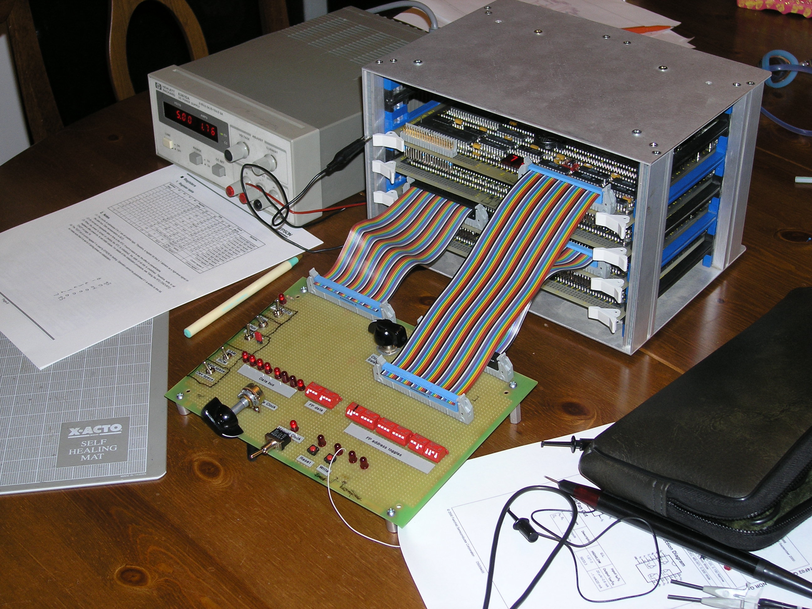
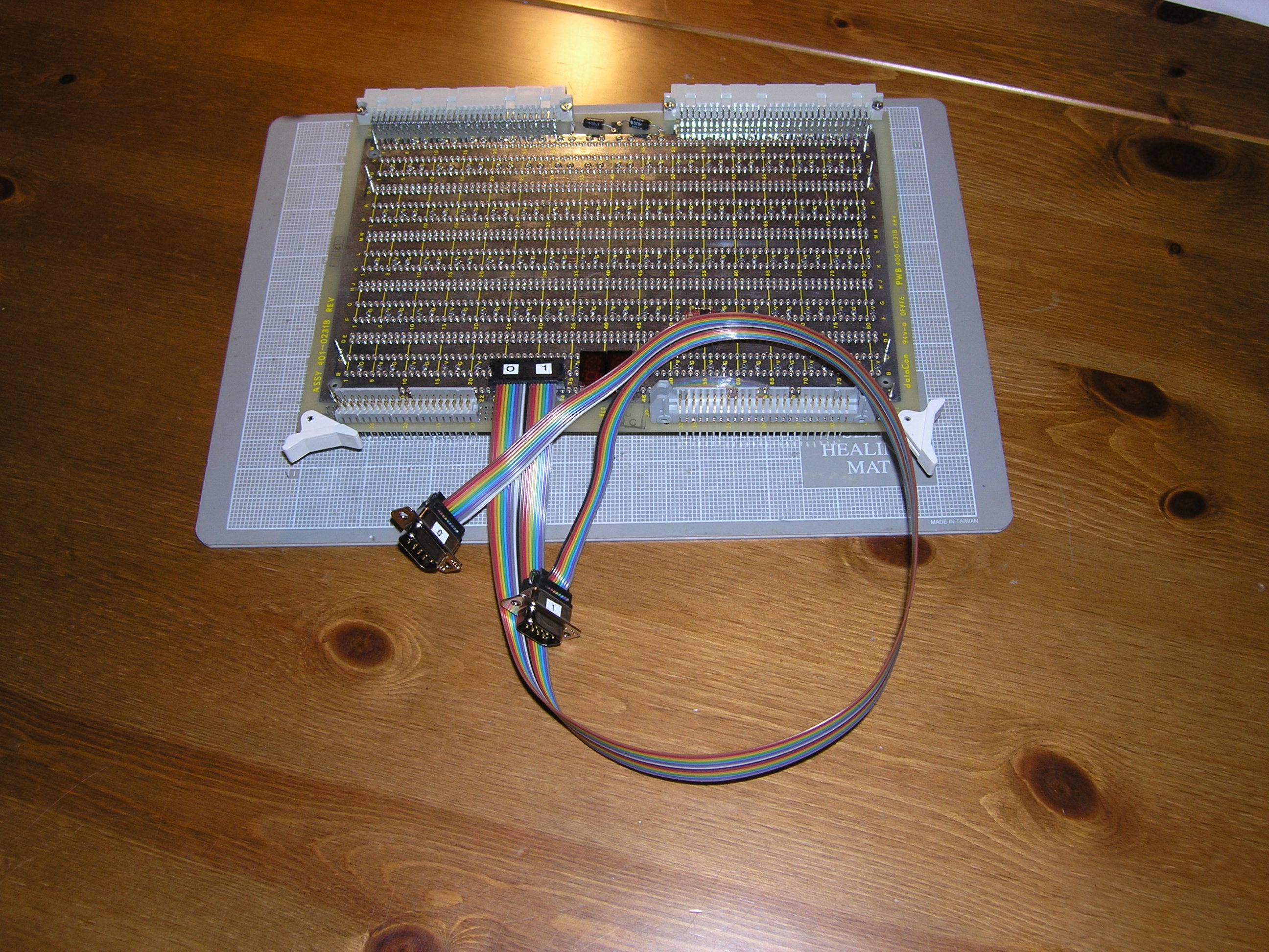
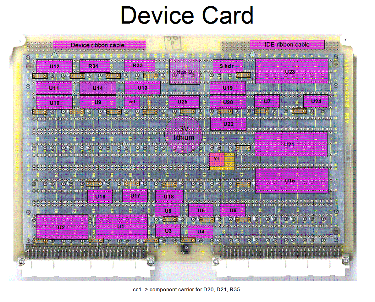
Device Card construction [completed 2/26/2004]2/26/2004Had to do a bit of rework related to device decoding, but everything looks good now. Ship it. 2/25/2004Things are looking good - it's starting to feel like a real computer. After fixing a couple of problems with bi-directional data bus handling for the front panel data switches, I got some great testing in. I can read and write memory in both the memory and device spaces, can read the ROM, write values to the POST code hex display - and even verfied that the real-time clock, including battery backup, is working. Here's it running:
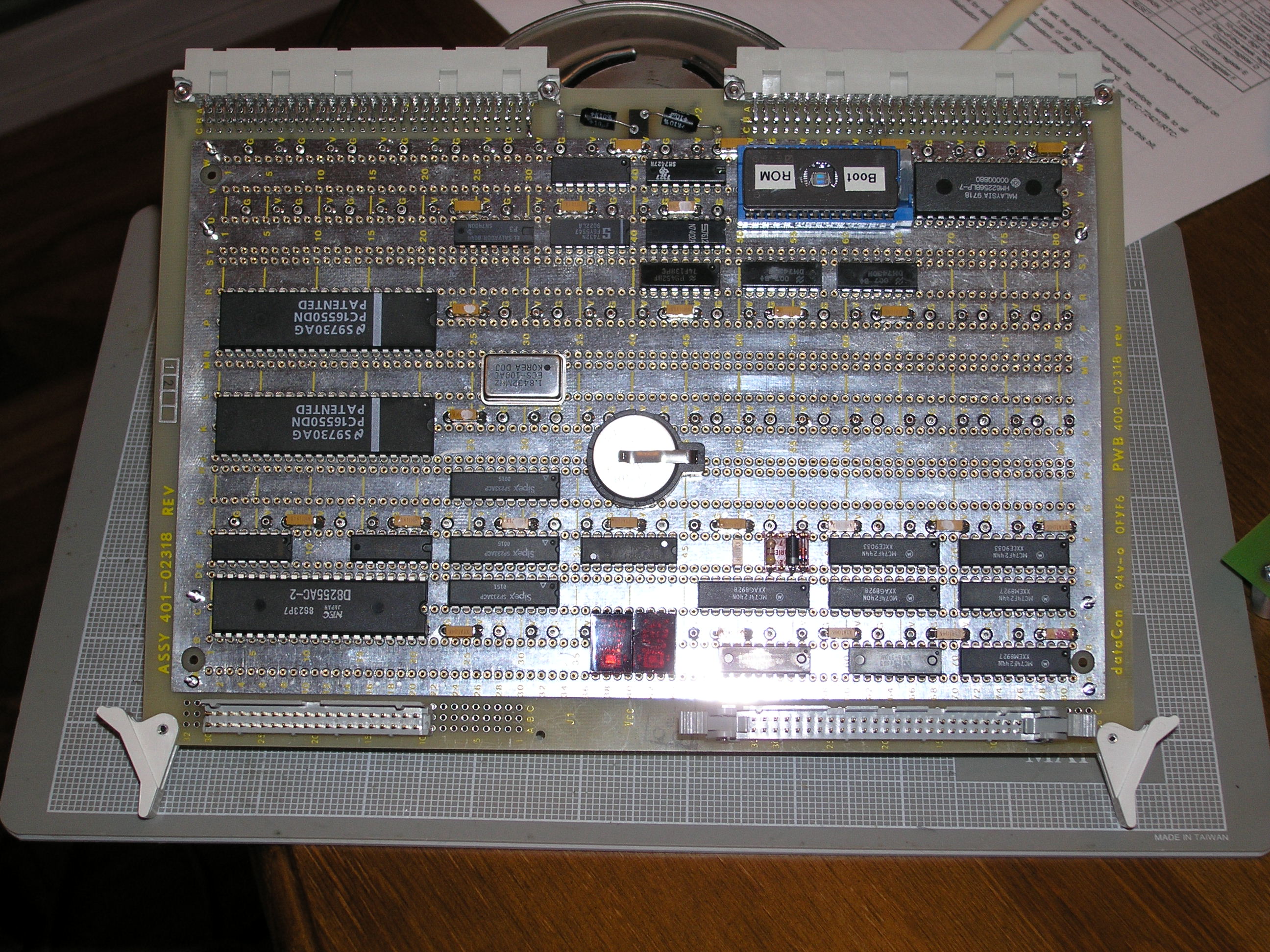
Notice that the cage has four cards now. There are a few signals that the control card generates that are necessary for really good testing. I went ahead and put a tiny bit of logic on a fresh card to supply these for testing. I did run into one particularly irritating problem - but then decided that it wasn't a bug, but a feature. It seems I got my orientation confused again with the HP hex displays for the POST code. The digits are swapped: least significant on the left, and most significant on the right. I've already wired those chips three times - and they are right in the middle of the data bus. Rather than wire it up for the fourth time, I've decided to declare it a feature. Magic-1 now boasts a "Hebrew Hex" POST code display (reads right to left...). Still need to figure out the new digital camera - most likely just set up a tripod and take pictures without the flash. But anyway, here's what the populated device card looks like:
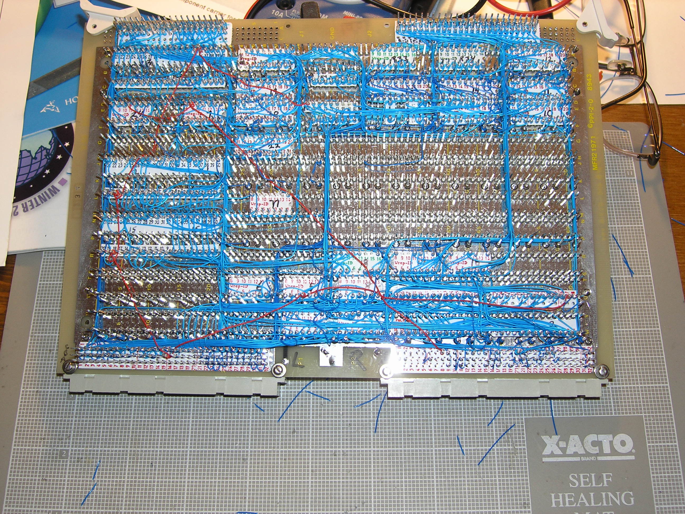
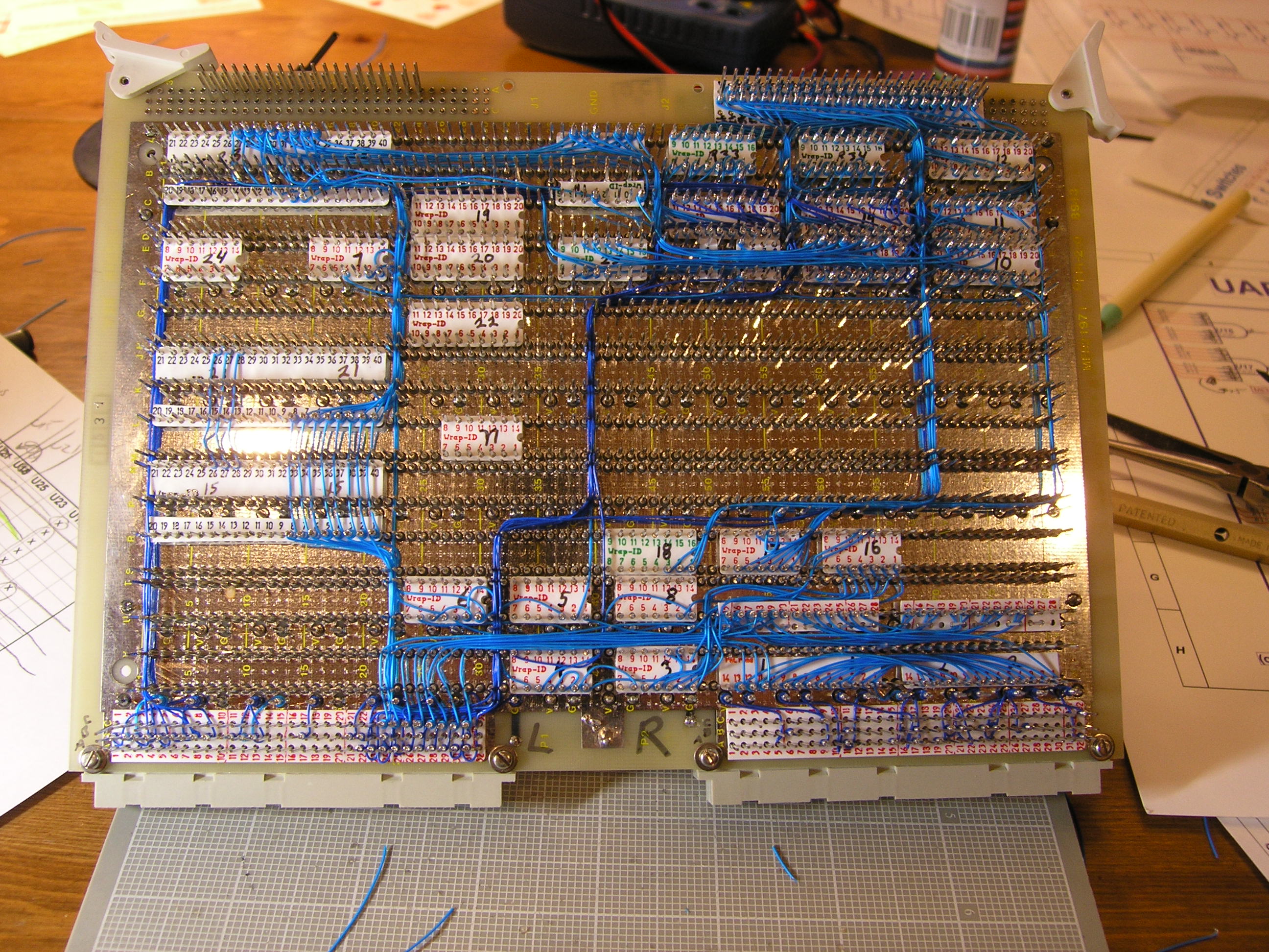
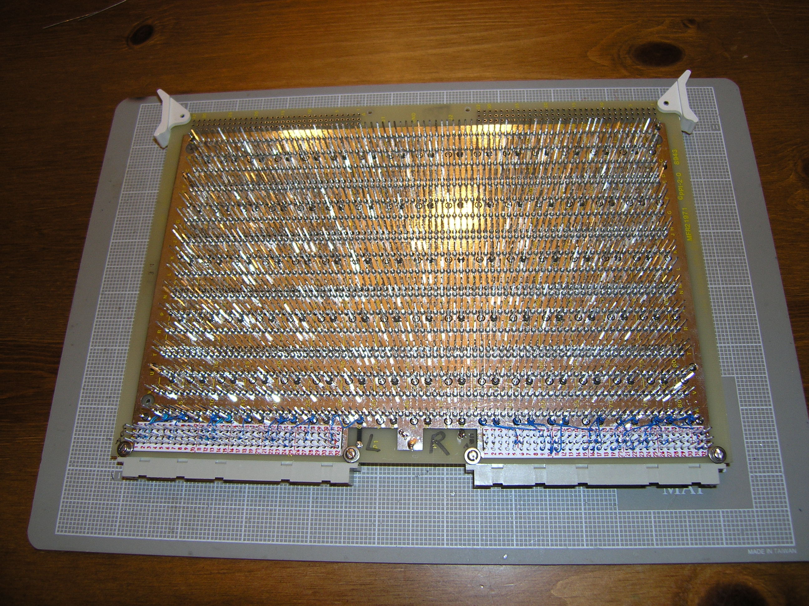
I'll guess that I'm another session or two away from completing testing. I want to pay particular attention to driving the address and data busses. After that, I'll declare this card complete and move on to the control card. 2/24/2004Long, long day working on the project. Probably too much time to spend in any one day. Anyway, beeped out all of the connections with my continuity probe. Found three problems, easily fixed. I also found what I thought was a problem, but was a bit too hasty. Seconds after I undid the suspect connection, I realized it was correct after all. Oh well. Not quite ready for power-on testing. I spent much of the day enhancing the temporary front panel assembly, and it's almost done. Getting close. 2/23/2004Finished the wiring of the device card, but lots of testing to do before I can call it done. Tommorow I'll beep out all of the connections with a continuity probe. For some reason, I really hate doing that, but it's necessary. Next up is adding another 50-line ribbon socket to the temporary font panel assembly, along with dip switches for the address and data lines, and a few LEDs to show the state of the data bus. Once that is done, I'll slowly start adding components to the device card - testing as I go. I'll have to be extra careful during this testing, as the device and memory cards can each drive the data and address busses. I'll need to make sure my drive logic is correct to keep them from hurting each other. The way it's supposed to work is that when a front panel switch is thrown, DMA_REQ is asserted. This is similar to an external interrupt line, and has no direct effect except on the microcode sequencer. When it's in a state to, the microcode sequencer will accept the DMA_REQ and then go into a tight microcode loop waiting for DMA_REQ to be deasserted. While in that loop, the microcode will assert DMA_ACK. DMA_ACK is the key signal that physically detaches the memory card's address and data bus drivers, while it at the same time enables the bus drivers associated with the address and data toggle switches on the front panel (whose circuitry is part of the device card). Anyway, for testing - because I don't have the control card up yet - I will have a toggle to manually assert DMA_ACK. I think I'll put in a jumper switch to disable the toggle when I start bringing up the control card. Once I have the front panel toggles working, I can manually address the EPROM, device SRAM, memory card SRAM, POST code displays, real-time clock and uarts. I don't plan on doing comprehensive testing on the devices, but enough to make sure I can address them correct and read/write control registers. Here's what the wire side of the device card looks line now:
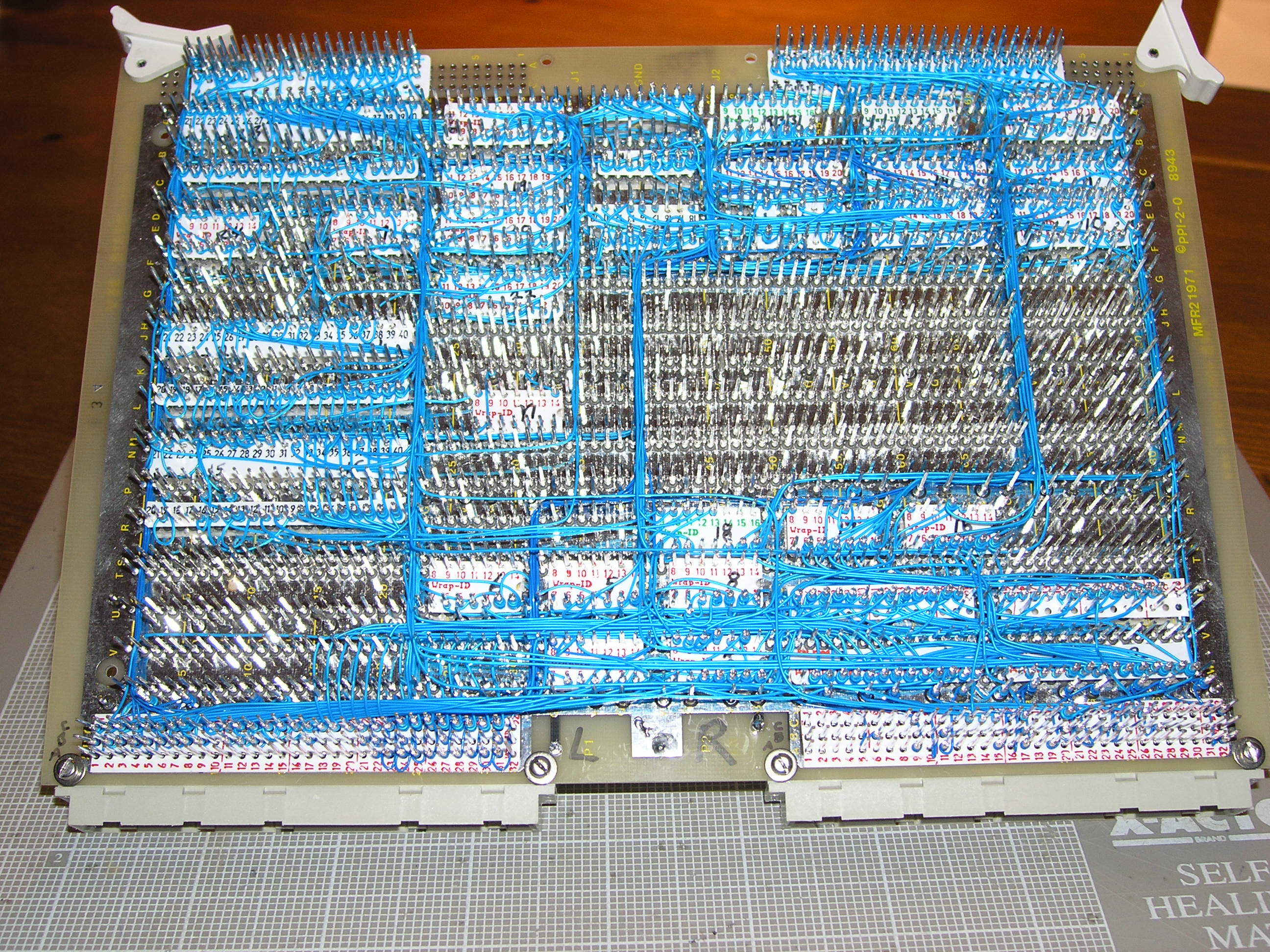
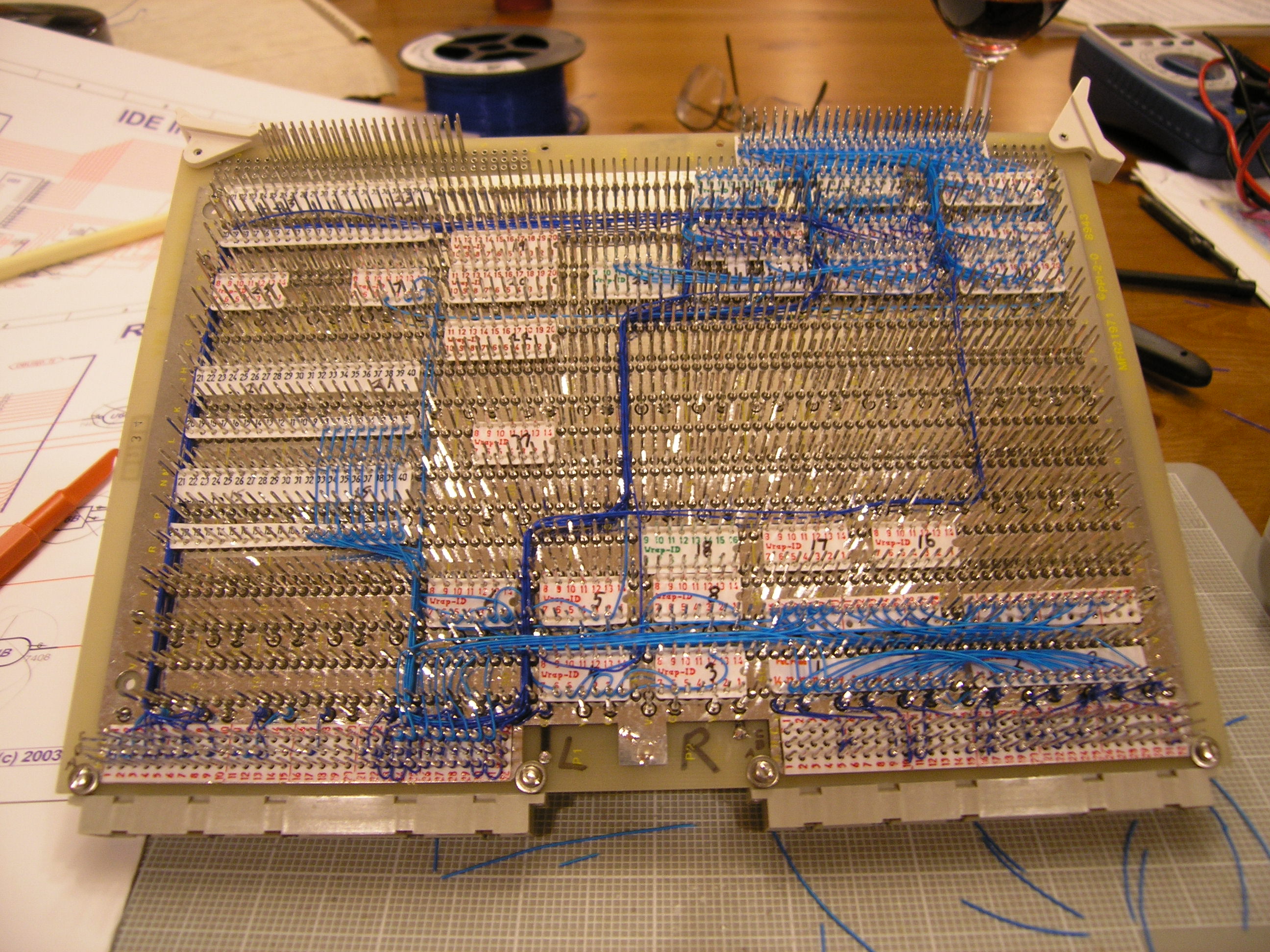
2/22/2004Almost finished with the device card. It turned out to be more difficult than I had expected. There was lots of irregular bus usage, and I ended up making two silly mistakes in the middle of the data bus (and had to redo some of the same wires twice). Also, I had to spend quite a bit of time trying to get my external cabling correct. What's left are the edge-sensitive lines, power/ground to all the devices and soldering in the bypass capacitors. Should take one or two work sessions. Here's what it looks like now:
Part of getting this far was wiring up the ribbon cable for the two serial ports. I am not particularly happy with what I ended up with - an 18-pin dip ribbon socket running off and splitting into two db9 connectors. I had hoped for an IDC header, but couldn't find any male pins that would work well with my wire-wrap board sockets. I fear breakage of the dip header if I have to plug it in and unplug it too many times. Guess I'll just have to be careful. Here's what it looks like. The header to the left is for the IDE drives, and the header to the right feeds a 50-line ribbon out to the front panel.
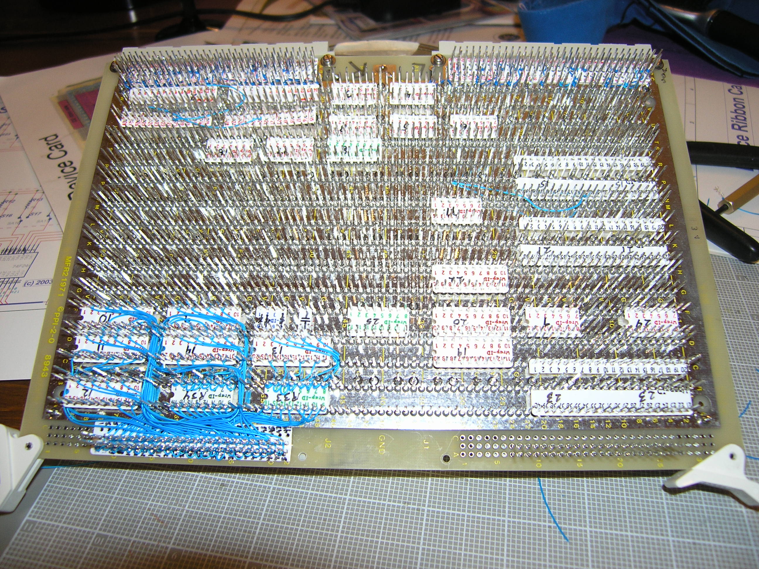
2/16/2004End of the three-day weekend; back to work tommorow morning. Got a lot accomplished on the device card. Finished up the data bus wiring and then tackled the address bus. The address bus is easily the most difficult part of this board. There are 22 address lines, and combinations of them touch 15 chips. I found it useful to create a spreadsheet showing which line touched which chip. This helped me visualize the wiring groupings, and from there dividing the 22 lines into 10 similar groups. Each of these was then split into bottom wire pairs, and top wire pairs. Spent a lot of time on this, and it worked out well. I've got 50 wires to go to finish off the address bus, and probably an additional hundred or so to finish off the card. After that, I have quite a bit of work to do on the temporary front panel logic card. To test the device card (and complete the memory card testing), I'll need the toggle switches and a bunch of LEDs installed. So far, it looks like I'll meet my goal of being in position to start on the control card the week of Feb. 20. Here's what the board looks like now:
2/15/2004Lots of wires in today. I've finished off the drivers for the MAR display that will go out to the front panel, as well as about half of the DBUS wiring. Finding and fixing minor mistakes from the schematics along the way. The potentially worst ones had to do with the way I've been correcting the bit numbering errors that the folks who designed the TTL chips made. For some reason, they consistently order bits wrong. All of the TTL devices show "0" as the low order bit, and then count upwards for higher-order bits. As right-thinking people know, bits and bytes are numbered starting with the big end: bit 0 and byte 0 are high-order, not low order. So, in my design, I number the bits in my busses correctly, and have to take care to account for the misguided little-endian numbering on the devices. Most of the time this doesn't matter, so long as I'm consistent. However, I discovered that I had ordering mismatches on my data bus bits where they hooked up to the 8255 that's part of the IDE drive circuitry. Glad I noticed - it would not have worked they way I had it (or at least my software drivers would have had to transpose all command and data bits heading out to the drive). One other irritating mistake - completely mine. When I did layout, I confused my "left" and "right" backplane bus connectors. This lead me to group some devices near the wrong bus connector. No real errors here, but it means I'll have a few longer wires that I would have otherwise. My big lesson here, though, is that naming things "left" and "right" is really stupid. When I did this, I had a solid mental image of the orientation of the boards, so it seemed natural. However, after constantly flipping the boards over, to the side, etc. while wrapping, I've lost any sense of "natural orientation". Should have named them B1 and B2 or something like that. Anyway, here's what things look like tonight:
2/14/2004Added the wire-wrap ID's and had a really good wrapping session - very few snapped wires. There was one problem: I made a mistake starting out the wiring of the toggle switches for the address bus. I started off wiring A0 into A1's position, and then continued my one-off error for the rest of the bus. Didn't catch it until the end. Rather than rip all the wires out, I decided to make the schematics reflect what I did. Wrapping regular patterns is nice, but you've really got to make sure you start off correctly. Anyway, no real harm done this time. Here's what it looks like so far:
2/14/2004 (afternoon)Finished up the layout. I'll do the wire-wrap ID's tonight, along with the headers.
2/11/2004Haven't finalized on the layout yet, but decided to go ahead and prep the board. I added the bus power/ground lines, the 10uF caps and some test pins for Vcc and gnd. Here it is:
2/9/2004Starting to think about device layout. This card will be notable for the large number of .6 devices - both 40 and 28-pin. It will feature one 60-line ribbon cable to the front panel assembly, as well at a 40-line IDE drive cable and 2 9-line serial port ribbons. Additionally, it will contain two old HP hex LED displays for POST code output - and I want to try to place those so I can see them from the outside of the cage. That might not be possible or easy, so I'll likely have to run a header or one of those ribbon-cable socket thingees. Bottom line - this card has a lot of stuff coming out of it. It's also heavy on A-bus and D-bus usage, and I'm thinking about avoiding my wire bundle channels. |